
In the RF and wireless industries, system performance requirements seem to expand almost daily. These systems continue to encompass more and more of today’s broad-reaching technologies. Engineers working in this environment are often tasked with designs that must combine and distribute RF signals from multiple input devices while, at the same time, making those signals available via multiple outputs. In many cases, an RF matrix switch can be the solution to this problem. In this article, the three most basic types of matrix switches are explored. The inherent advantages and disadvantages of each of these configurations will also be touched upon.
Blocking Matrix

A blocking matrix switch is built with switches on both the inputs and outputs. Therefore, each input signal can be switched to one individual output port. If an application requires an input to be available to more than one output simultaneously, then a non-blocking matrix becomes necessary.

Figure 1 shows the connectivity of a 3 × 3 blocking matrix switch. Figure 2 depicts some of the possible connection states with this type of switch. The two most notable advantages of a blocking matrix switch are insertion loss and isolation. Because the design uses only switches and no power dividers, the insertion loss is relatively low. Using only switches makes it also possible to maintain a very high isolation from input to output. However, one significant disadvantage to this type of design is its cost. RF switches are generally more expensive to produce than RF power dividers.
Non-Blocking Matrix
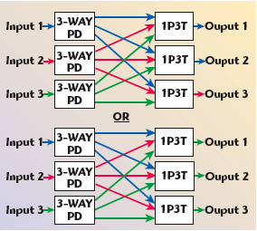
A typical non-blocking matrix switch is one that is built with power dividers on the inputs and switches on the outputs. Each input signal is thereby split to all output switches. This means that, in a 4 × 20 non-blocking matrix switch for example, the four input signals could be split to all 20 outputs. This would allow an engineer to select the signal to be seen at each output. Or a user could even have a single input connected to all 20 outputs without even using the other inputs. Figure 3 shows the layout of a typical 3 × 3 non-blocking matrix.

Figure 4 depicts some of the possible connection states with this type of switch. The obvious advantage of a non-blocking matrix switch is its greater switching flexibility. However, certain compromises have to be made in order to achieve that increased flexibility. Because it uses power dividers, a matrix like this will have a higher nominal insertion loss. Having a power divider at each input can also have a negative effect on the isolation between channels. In the event that two outputs are switched to receive the same input signal, the isolation between output ports is determined by the isolation of the power divider. Typically this will be approximately 20 dB.
Non-blocking Matrix — Extended Variation
An extended variation of a non-blocking matrix switch is one that is built with power dividers on the inputs and outputs. Depending on the functionality needed, an array of either 1P1T switches or programmable attenuators is placed between the layers of power dividers. This configuration allows for multiple input signals to be available at one output. When the programmable attenuator option is exercised, a user may individually adjust the strength of each signal being received by an output.
Figure 5 shows a 3 × 3 extended variation non-blocking matrix. Figure 6 shows some of the connection states and manipulations that are possible with this type of switch. This configuration offers even greater switching flexibility than a standard non-blocking matrix switch and can even be used bi-directionally. Once again, however, this configuration does have its disadvantages. Using twice the number of power dividers results in an even greater nominal insertion loss through the system.

When choosing the right matrix switch design, it is important to have a thorough understanding of the application. Many different variables must also be taken into account, along with the matters of connectivity that were addressed in this article. Everything from RF performance and reliability to control interfaces and programming should be considered before making a decision.
