
For more than 15 years, Spectrum SEI Microwave has developed PIN diode and MMIC-based switched filter banks. Recent advancements have made micro-electromechanical systems (MEMS)-based RF switches advantageous for particular applications. The model 310-020022-001 is SEI’s first MEMS-based switched filter bank.
Switching
The company was presented with a need for a 9-channel amplified switched filter bank with the lowest possible current consumption while maintaining high linearity over a multi-octave bandwidth. Additionally, the application did not call for continuous switching, as the filter bank required operation in a particular frequency band for relatively long periods of time. Given these criteria, the most logical switching solution would be some type of latching mechanical relay that does not draw current to maintain its state.
The use of conventional latching mechanical RF relays could be quickly eliminated due to two primary shortcomings. With high levels of stray capacitance, a binary tree switch structure would be required to achieve broad bandwidth. The use of a binary tree structure, as shown in Figure 1, leads to high insertion losses as the resulting circuit has a minimum of six switches per path. Conventional relays are also relatively large in size.

Fig. 1 A binary tree structure.
The model M1C06-CDK2 RF MEMS switch developed by Magfusion is a miniature latching SPDT relay that has many characteristics that make it an excellent choice for this application. With low insertion loss and low stray capacitance, the MEMS switch offers flexibility in configuration of the switch matrix. Depicted in Figure 2, the final switch configuration is best described as a hybrid radial-binary tree. The common arm incorporates a low pass structure to absorb the cumulative stray capacitance from the radial portion of the switch matrix. To keep losses low, the five highest frequency bands have only four switches per path. The lower bands can tolerate a higher number of switches per path since the filters and the switches exhibit less loss at lower frequencies.

Fig. 2 The hybrid radial-binary tree configuration.
Technical Challenges and Solutions
The need to minimize power consumption presented challenges throughout the design process. Because it is magnetically self-latching, the M1C06-CDK2 switch eliminates the need to expend energy to maintain a selected switch state. This allows for all logic and control circuitry to be powered down when the user is not commanding a state change. When the filter bank is in a set-on mode, the channel amplifier is the only device drawing current. To accommodate a logic power-down, an eclipsing pulse is used to initiate a state change. The eclipsing pulse is asserted when the user has established a valid 4-bit TTL control word specifying the desired frequency band. Figure 3 illustrates the logic timing.

Fig. 3 Logic timing of the eclipsing pulse.
Another useful aspect of the M1C06-CDK2 switch is its ability to withstand hot switching. The device is rated at 100 million cycles for a bias condition of 10 V and 10 mA. This property allowed the amplifiers’ supply voltages to be applied to the common arm of the 9-pole input switch matrix and subsequently drawn off the ON arm. As a result, no additional control circuitry was needed to power the channel amplifiers ON and OFF.
Although the MEMS switches do not require power to maintain their switch state, each device typically draws 110 mA for approximately 200 ms to toggle its state. With 18 MEMS switches per filter bank, this switching current could quickly add up to a significant load on the power supply if all switches had to be commanded when a new tuning word was loaded. Several techniques were employed to minimize the switching current. If the existing state of the filter bank is known when the user initiates a change to a new desired state, then it can be determined which MEMS switches require toggling and which do not. The technique of hot switching the amplifier supply voltage through the MEMS switches, as previously discussed, presented a unique solution to the challenge of storing the existing state without consuming additional current. By sensing which arm of the input switch matrix holds the supply voltage, the existing state could be determined. This information is digitally processed through a complex programmable logic device (CPLD) that determines which MEMS switches must be toggled based on the new desired state.
Capacitive energy storage is also used to minimize the switching current draw required from the power supply. Due to size constraints, an array of discrete tantalum capacitors combines for nearly 4000 mF. Additional energy storage is obtained through the use of power and ground planes formed on inner layers of the PC board.
The mechanical requirements for this filter bank also presented several design challenges. To accommodate all the necessary control circuitry, a 4-layer PC board was used with both top and bottom layers fully populated. Using a total of 18 MEMS switches made it inevitable that several devices would be in close proximity to each other. This close proximity presented an assembly challenge when switches began repelling each other due to their strong magnetic fields. A custom assembly fixture was fabricated to hold the components in place during reflow. It should be noted that the M1C06-CDK2 switch is now available in a magnetically shielded package, which will reduce the observed effects.
Performance and Construction
The model 310-020022-001 is an amplified switch filter bank consisting of nine selectable RF frequency bands covering a range of 20 to 500 MHz. The critical performance parameters for the 310-020022-001 unit are listed in Table 1. Small signal gain is 15 dB while drawing just 8 mA typically from a single +3.3 VDC supply. Each of the nine channels exhibits an 8-pole Chebychev filter response. A typical transfer function is depicted in Figure 4. The unit is designed with a filter-amplifier-filter configuration offering low distortion amplification of the input signal.


Fig. 4 The switch filter bank’s typical transfer function and return loss.
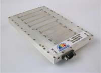
The complete assembly is housed in a rugged 4.65" × 3.00" × 0.40" machined aluminum chassis with a silver plate finish and through-hole mounting. RF connectors are SMP-male, while power and logic signals are externally applied through a 9-pin micro D-sub connector.
Conclusion
Although not suitable for continuous switching applications, MEMS-based switch banks offer several advantages over PIN diode versions. A passive version is under development that consumes zero power while operating after the commanded state is reached. In a passive switched filter bank, latching MEMS switches would also provide a fail-safe for operation in case prime power is lost. Another advantage is the linearity of the MEMS over PIN diodes. A passive MEMS-based switch bank is able to handle in excess of 30 dBm, while a PIN diode version with only a 3.3 V supply would be limited to approximately 18 dBm unless DC-DC converters were used.
The 310-020022-001 switch filter bank has begun to tap into the advances in MEMS switches and their applications to RF and microwave systems. This concept could be extended to higher frequencies with various channeling configurations for either passive or active applications.
Spectrum Microwave,
Delmar, DE
(302) 846-2750,
www.specwave.com.