
UltraSource is a high quality supplier of precision thin film circuit fabrication including custom resistor networks and attenuators, metallized substrates and MEMS fabrication with a focus on using its thin film manufacturing capabilities to supply custom products from prototypes to high volume production. The products range in application from wireless communications, DC to 200 GHz microwave components, fiber optic and laser technology, infrared imaging systems, microwave calibration and test fixtures, and other commercial and military products.
Recently the company has added multi-layer thin film interconnect technology to its list of capabilities. This new technology is specifically designed for high yield manufacturability and reliability. Multi-layer thin film interconnect technology reduces assembly time and improves yield and manufacturability, while improving performance and repeatability. It increases circuit density while reducing the number of wire bonds, and enables high frequency design with 10-micron lines and spaces. At the same time the process lowers material content and cuts cost.
The Ultra process offered incorporates the deposition of a thin layer of silicon nitride Si3N4 as a dielectric layer to facilitate metal-insulator-metal (MIM) layered structures on a substrate, thus making a very robust structure with increased reliability and repeatable performance. The process can be used to create circuit bridges, and realize RF capacitors and high Q inductors.
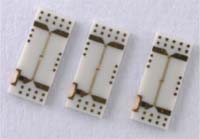
UltraBridge structures create dense, fully integrated solutions to complex interconnect challenges such as in fabricating Lange couplers and multi-chip modules. It is a cost-effective alternative to air bridges. Figure 1 shows an example of an UltraBridge utilization.

Fig. 1 An UltraBridge utilization.
UltraCapacitor structures form integrated capacitors for dense circuit areas. These capacitors are available in values from 2 to 250 pF with tolerances of 10 percent. They are ideal for use in next level integration of passive elements. Figure 2 shows an example of UltraCapacitors.

Fig. 2 An example of UltraCapacitors.
UltraInductor structures facilitate high Q spiral inductor designs, thereby reducing large wire bonds and associated parasitic inductances. Figure 3 demonstrates typical UltraInductor use.

Fig. 3 An UltraInductor structure.
The Ultra process is comprised of a base conductor of TiW/Au and a dielectric of Si3N4 with a dielectric constant of 7.8, providing a capacitance density of 0.05 to 0.15 pF/mil2. The substrate material is Al2O3 /AlN.
Ultra process structures are currently being used in everyday products such as wireless communication systems and microwave components. The process offers a robust solution with increased reliability and lower costs.
UltraSource Inc.,
Hollis, NH
(603) 881-7799,
www.ultra-source.com.