The HMC670LC3C 1:2 Fanout Buffer uses differential inputs and outputs which are DC coupled and terminated on chip with 50 Ohm resistors to ground. The outputs may be used in single-ended or differential modes. With typical rise and fall times of 24 and 22 ps, and 1 ps of deterministic jitter, while dissipating only 240 mW.
The HMC671LC3C, may be configured as either an XOR or XNOR logic function, and the HMC672LC3C may be configured to provide AND, NAND, OR or NOR logic functions. Both devices use differential inputs which are terminated with 50 Ohms to ground on chip. The differential inputs and outputs of the HMC671LC3C and the HMC672LC3C may be either AC or DC coupled. These devices exhibit a propagation delay of 60 ps, rise and fall times of 24 and 22 ps, and 1 ps of deterministic jitter while dissipating only 180 mW.
HMC673LC3C, D-Type Flip Flop supports both positive and negative edge triggering and inputs to the device may be either AC or DC coupled. The differential outputs may be either AC or DC coupled and propagation delay is typically 55 ps. The HMC673LC3C typically provides rise and fall times of 24 and 22 ps and 1 ps of deterministic jitter while dissipating only 210 mW.
The HMC670LC3C, HMC671LC3C, HMC672LC3C and HMC673LC3C support data transmission rates up to 13 Gbps, and clock rates up to 13 GHz. These devices feature an output level control pin which enables signal level optimization by allowing the output voltage swing to be adjusted between 0.4 and 1.1V. These devices operate from a single -3.3V DC supply, are housed in ceramic 3x3 mm SMT packages. Released data sheets are available on-line at www.hittite.com
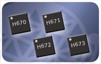
HMC670LC3C, HMC671LC3C, HMC672LC3C and HMC673LC3C