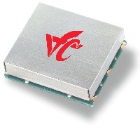
VFJA905 Jitter Attenuator

While Synchronous Optical Networks (SONET) have been widely adopted for use in long-haul applications, Ethernet is preferred in edge routers and access points due to its lower cost. Ethernet is a packet-based network architecture that is asynchronous, while SONET networks are synchronous. Hence, the two networks cannot communicate seamlessly with each other, representing a significant operating problem. The solution is Synchronous Ethernet (Sync-E). Sync-E makes it possible to connect synchronous and asynchronous networks using point-to-point connections (see Figure 1). Fig. 1 A 1 GigE solution using the VFJA905 jitter attenuator. With any transmission system that carries its own synchronizing timing signal over long distances, bit error rates increase due to the degradation of the synchronizing clock signal. Thus, the elimination of jitter associated with the clock signal is critical to successful operation of such a system. Valpey Fisher introduced the Jitter Attenuator for both Single GigE and 10G applications to meet this requirement. The recently introduced VFJA905 Jitter Attenuator provides two LVCMOS outputs with a frequency of 25 MHz that can be locked to an input reference frequency. Two select inputs, S1 and S0, allow the user to select one of three preset input frequencies or a free-run mode. In free-run mode the device outputs a 25 MHz clock that is not locked to the input reference frequency. In the synchronized mode the VFJA905 unit receives its reference clock typically for a downstream recovered clock. It then attenuates the jitter in the recovered clock signal and provides the Master PHY with an ultra-low jitter sync clock signal. The slave PHY recovers the clock, which becomes the reference for the VFJA905, which in turn provides the reference clock to the next master PHY. Fig. 2 Typical jitter transfer gain. Figure 2 shows the VFJA905 unit’s typical jitter transfer gain and phase response. At approximately 10 Hz the jitter transfer gain is –10 dB. At 1 kHz and beyond the jitter is attenuated to negligible levels. The VFJA905’s jitter bandwidth is much lower than that of the Ethernet PHY; therefore, the combined jitter transfer gain is dominated by the Jitter Attenuator. The OC-48 specification requires a maximum wideband jitter of 80 ps peak-to-peak. Figure 3 shows an eye-diagram of a PHY with the VFJA905 in operation. The wideband jitter is 56.7 ps peak-to-peak, providing ample margin. Figure 4 displays the VFJA905 jitter attenuator’s block diagram. Fig. 3 An eye-diagram of the PHY with the VFJA905. It represents a single device solution that requires no external reference oscillator. It features ultra-low output jitter (sub 0.18 ps RMS) and is compliant with GR-253-CORE, GR-1244-CORE, ITUT-G.813 and ITUT-G.8261. With its user-selectable free-run mode the device can set to run either as a stand-alone device or locked to the input. Multiple outputs eliminate the use of an external buffer. Also, with its selectable input the same device can be used for multiple applications. The VFJA905 operating specifications include a 10 to 200 MHz output frequency range, an 8 kHz to 200 MHz input frequency range, and ultra-low jitter and phase noise (0.18 ps RMS and –143 dBc/Hz at 1 kHz). The device operates from a +3.3 V DC power supply and typically consumes 150 mW. The VFJA905 is available in a 19.5 x 15.5 mm surface-mount package and is RoHS 6/6 compliant.
