
Electromagnetic bandgap (EBG) materials are periodic structures that exhibit wide bandpass and band rejection properties at microwave frequencies. Introducing periodic perturbations such as dielectric rods, holes and patterns in waveguides and PCB substrates forms photonic bandgap (PBG) materials. As in a photonic crystal (PC), photon propagation is impeded by electrons and the electromagnetic waves in a PBG material are impeded due to the periodic discontinuities, hence creating a slow-wave structure. Currently, people are also referring to the term PBG as EBG. Due to their unique properties, EBG materials find potential applications in antennas, waveguide, amplifiers, filters, power combining, phased arrays, EMC measurements and in many microwave devices. The application of PBG engineered materials causes the suppression of surface waves.1–7 Consequently, the performance of active and passive microwave components and devices is enhanced. The use of PBGs in the ground plane of a microstrip line provides attractive features.8–11 Even the PBG engineered microstrip line itself shows excellent and attractive performance.12 PBG may have many forms due to their different lattice structures. Their behavior can be controlled with the proper choice of different lattice structures and the lattice parameters.
Recently developed uniplanar compact photonic bandgaps (UC-PBG) are very useful for different applications.13 The passband characteristic of the UC-PBG is used as a slow-wave medium, which reduces the size of electronic circuits. The deep stopband is applied to suppress spurious transmission and leakage in guiding structures such as conductor backed coplanar waveguides (CB-CPW) and striplines. The use of PBG structures in antenna design provides better performance.14–21 Due to the superior performance of EBG assisted microwave devices, research on different EBG structures (EBGS) is accelerating exponentially.
This article reviews the EBG configurations and the application of EBG engineered structures in different microwave applications. In this context, the novelty of this structure has been explored for a high Q image guide resonator useful in the design of low noise oscillators,22 microcavities for better light emitting diode (LED),22 power amplifiers,23 low pass filters,24,25,26 bandpass filters13 and mixers.25 The comparison between EBG engineered and conventional structures demonstrates the importance of EBG materials in microwave engineering. It is believed that this novel structure has opened up a new era in the development of broadband and highly efficient microwave components and devices.
EBG Configurations
EBG structures are periodic in nature, and may be realized by drilling, cutting and etching the metal or substrates. They may be formed in the ground plane or over the substrate. A recent trend is where the main element such as the transmission line is itself creating a PBG12 without having any perturbation in the ground plane. This new idea can be extended to filters, antennas and other microwave components and devices where the important issue of packaging will be minimized. The PBG configuration can be categorized, as shown in the tree structure of Figure 1. On the basis of dimensions, PBG structures may be classified as 1-D, 2-D and 3-D PBG.
 | ||
| Fig. 1 PBG structure configurations. | ||
Bumpy Surface
Several configurations have been reported in the literature. The first structure is made by drilling a periodic pattern of holes in the substrates27 or etching a periodic pattern of circles in the ground plane.8 A bumpy surface is shown in Figure 2. A bumpy metal sheet has a narrow surface-wave bandgap. The electric field wraps around the bumps at the upper edge of the bandgap (a) and the electric field extends across the bumps at the lower edge of the bandgap (b); hence, a slow-wave structure is achieved.
 | ||
| Fig. 2 Bumpy metal sheet. | ||
Corrugated Surface
A corrugated surface,28 shown in Figure 3, is a metal slab into which a series of vertical slots have been cut. The slots are narrow, so that many of them fit within one wavelength across the slab.
 | ||
| Fig. 3 Corrugated metal surface. | ||
Each slot can be regarded as a parallel plate transmission line, running down into the slab and shorted at the bottom. If the slots are one quarter-wavelength deep, then the short circuit at the bottom is transformed by the length of the slots into an open circuit at the top end. Thus, the impedance at the top end is very high.6 In this situation, the surface impedance is capacitive and transverse magnetic (TM) surface waves are forbidden. Furthermore, a plane wave polarized with the electric field perpendicular to the ridges will appear to be reflected with no phase reversal.
Metal Pad or High Impedance Surface
A more effective and compact approach, which makes use of a triangular or square lattice of metal pads connected to ground with vias, has been recently proposed2,6 and can be applied to enhance the gain of planar antennas. These structures are the first realization of planar compact electromagnetic crystals with a complete stopband in the microwave range. This type of textured structure with a triangular lattice of hexagonal metal plates that provides high impedance surface is shown in Figure 4.
 | ||
| Fig. 4 High impedance surface; (a) cross-section and (b) top view. | ||
Planar PBG
The periodic structures are etched in the ground plane. They may be of different forms on the basis of a lattice structure,10 which may be square, triangular, rectangular, honeycomb, etc. The shapes of the unit cell10,29 may also be square, rectangular, circular, triangular and sinusoidal, etc. A continuous research effort is being made to develop different PBG structures to obtain the required performance. Planar slow-wave structures and low leaky conductor-backed coplanar waveguide using a UC-PBG substrate (Figure 5) have recently been presented.16 In a UC-PBG, vias are not used. Advantages of this crystal are its simple and low cost configuration compatible with MMICs. The UC-PBG structure is a two-dimensional periodic lattice pattern on a conductor-backed dielectric substrate. The unit cell of the PBG lattice consists of square pads and narrow branches, which have an inductive behavior that is further enhanced by insets.
 | ||
| Fig. 5 UC-PBG geometry; (a) substrate and (b) unit cell. | ||
The PBG structure forms a distributed LC network with specific resonant frequencies. At these frequencies, the periodic loading becomes an open circuit and an equivalent magnetic surface is created. Very recently, a new simplified UC-PBG has been proposed by S.K. Sharma and L. Shafai.30 It reduces cost with better performance in antenna applications.
The authors have proposed a ring PBG structure24 that is a potential candidate for more freedom because of its extra aspect ratio characteristics. By changing the aspect ratio of the structure, the bandgap and bandwidth can be controlled. A recent contribution of the authors31 includes the concept of non-uniform distribution of PBGs to be used as a low pass filter (LPF) with improved performance. The authors also propose non-uniform ring PBGs by which the passband ripple is dramatically suppressed both at higher and lower frequencies.
Thus far, different PBG configurations have been presented. The following sections highlight the revolutionary possibilities afforded by PBG integration in RF and microwave electronics.
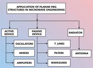
Microwave Applications of EBG
PBG engineered structures find many applications in microwave components and devices due to the unique properties. To realize microwave filters, mixers, antennas, power amplifiers and phased arrays, etc., the stopband and passband created by the PBG structures play a vital role. After a comprehensive literature review, the applications of EBGs have been categorized, as shown in Figure 6.
 | ||
| Fig. 6 Applications of planar PBG structures. | ||
Low Noise Oscillator Design
Y. Qian, et al.22 offer the design of PBG engineered passive and active components. Application of a high Q image guide resonator results in a low noise oscillator. The defected mode concept in PBG structures has been utilized here. The schematic of a high Q resonator based on PBG defect-effect in an image guide is shown in Figure 7, where a is the period of the 1-D lattice of grooves. It is interesting to note that a stopband for wave propagation is achieved when Bragg’s condition24 is satisfied. On the other hand, a sharp high Q defected mode can be obtained when a cavity is formed in the middle of the PBG lattice with a length l. A modulated Gaussian pulse outside the PBG grooves excites the image guide. In this case, 8.255 GHz is obtained as the peak frequency for transmission.
 | ||
| Fig. 7 A high Q image guide resonator. (See Ref. 22, © 1998 IEEE) | ||
An experimental investigation is needed for the design of a proper coupling scheme to launch and measure the image guide mode. A microstrip-fed Yagi-Uda slot array is used in the design of an efficient transition (as shown in Figure 8) that is used for the measurement of “S-parameters.” It can be seen from the result shown in Figure 9 that the peak frequency is 8.276 GHz, which is excellent (only 0.25 percent error). A reasonably high value of unloaded Qu of 697 is measured. In a low noise oscillator design, this type of image guide resonator is a potential component to provide a relatively pure spectrum. Figure 10 shows how the resonator is used to realize a low noise oscillator. The resonator provides an output power level of 8.5 dBm after subtracting the coaxial cable loss. A noise level of approximately –102 dBc/Hz at 100 kHz offset is obtained. The image guide resonator is used in the feedback loop of a cascaded amplifier.
 | ||
| Fig. 8 Image guide resonator fed by microstrip lines and Yagi-Uda coupling slot arrays. (See Ref. 22, © 1998 IEEE) | ||
 | ||
| Fig. 9 Measured S-parameter of the image guide resonator. (See Ref. 22, © 1998 IEEE) | ||
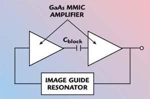 | ||
| Fig. 10 Schematic of a low noise oscillator with a high Q image guide resonator in the feedback loop. | ||
Enhanced Spontaneous Emission Led by Microcavities
PBG based microcavities22 provide an LED with enhanced spontaneous emission. In the terahertz frequency range, the PBG-based microcavities are outstanding candidates to achieve single mode, small volume resonators. These types of cavities are used to enhance spontaneous emission and to increase the efficiency of an LED. In Figure 11, a high dielectric slab resides on a substrate with a much lower value of dielectric constant so that the electromagnetic energy of the guided modes is confined inside the high dielectric constant slab.
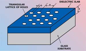 | ||
| Fig. 11 Upper substrate perturbed by a triangular lattice structure of circular PBGs. | ||
The dispersion diagram of a transverse electric (TE) like mode, shown in Figure 12, is for t/a = 0.33 and r/a = 0.40, where t is the thickness of the substrate, r is the radius of a circular-patterned EBGS and a is the inter-element distance. A bandgap for the guided propagation is found in the range of 0.33c/a to 0.4c/a only for TE-like modes, where c is the velocity of light.
 | ||
| Fig. 12 Dispersion diagram of a TE-like mode originated from Figure 11. (See Ref. 22, © 1998 IEEE) | ||
Defects realized by adding an appropriate volume of dielectric material are necessary to support highly localized electromagnetic modes, whose frequency will fall within the range of the forbidden gap of the two-dimensional crystal. The energy of these modes cannot couple to the guided modes of the slab; it resides around the defect, which acts as a microcavity. In the design of light emitting diodes, it is an excellent component where the energy is confined in the active region of the LED. Three configurations are shown in Figure 13, where the minimum effective volume is about 2, in units of (λ/2h)3, for all configurations. Y. Qian, et al.22 suggest that this value is expected to achieve a five-fold spontaneous emission enhancement. The smallest possible EM mode volume in a dielectric cavity has been previously documented.23 The performance of PBG-based microcavities to provide enhanced emission of LED is shown in the figure.
 | ||
| Fig. 13 Performance of PBG-based microcavities to provide enhanced emission of LEDs. (See Ref. 22, © 1998 IEEE) | ||
Suppression of LO Leakage in a Mixer
A conventional low pass filter (LPF) needs many stages to reject the LO leakage. However, a UC-PBG-structured filter can be used to suppress this leakage in a mixer, as shown in Figure 14. The UC-PBG filter25 is placed at the drain side to extract IF output as well as to reject the LO leakage. Figure 15 shows the comparison of conversion gain and LO leakage between a PBG assisted mixer and a conventional mixer. The graph shows that the LO power has been injected into the drain more efficiently from the increase in conversion gain from 1 to 1.5 dB at lower levels when using the PBG filter. It is very clear that the PBG mixer suppresses the LO leakage by more than 10 dB.
 | ||
| Fig. 14 Layout of a mixer with a UC-PBG structure. (See Ref. 25, © 1999 IEEE) | ||
 | ||
| Fig. 15 Comparison between a PBG assisted mixer and a conventional one; (a) conversion gain and (b) LO leakage. (See Ref. 25, © 1999 IEEE) | ||
Broadband High Efficiency Power Amplifier
The achievement of broadband harmonic tuning is typically cumbersome for active integrated antenna amplifiers and for power amplifiers in general. The technique of using a periodic structure is actually well suited for a narrow band. Thus, additional harmonic filtering is required that necessitates larger transmission stopbands. These types of larger stopband filters can be achieved with the use of PBG ground plane. The proposed PBG ground plane for microstrip lines32 provides low loss, slow-wave propagation at lower frequencies and a wide distinctive stopband as the frequency increases.9,26 The implementation of a PBG ground plane in power amplifiers results in intrinsic, broadband harmonic suppression without any stub or filtering element. In the design of broadband power amplifiers the PBG periodic structure is integrated with a slot antenna, where it is used to tune the second harmonic. The measured input impedance of the slot antenna with a microstrip feed is shown in Figure 16. It has been mentioned by V. Radisic, et al.32 that the measured power added efficiency (PAE) is better than 50 percent over an 8 percent bandwidth (3.7 to 4.0 GHz) with second harmonic tuning only. When a combined approach,32 where a microstrip patch with shorting pins is used to tune the second harmonic and the periodic structure is used to tune out the third harmonic for a class AB power amplifier, the PAE is 61 percent with an output power of 21.9 dBm.
 | ||
| Fig. 16 Performance of a PBG structure integrated with a slot antenna. (See Ref. 32, © 1999 IEEE) | ||
Efficient Transmitter Front-ends Integrated with EBG
The tuning of second and third harmonics provides an efficient power amplifier. C.Y. Hang, et al.33 show a comparison between an amplifier assisted with a PBG microstrip line at the output, and a reference amplifier with a standard 50 Ω microstrip line of identical length. The measured and simulated PAE versus input power for the PBG and reference amplifier at 3.6 GHz are shown in Figure 17.
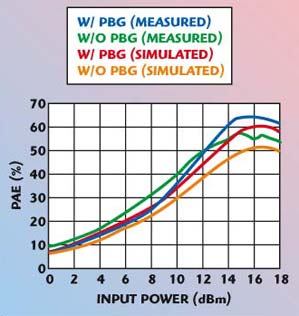 | ||
| Fig. 17 Measured and simulated performance of an efficient transmitter front-end with and without PBG. (See Ref. 33, © 2000 IEEE) | ||
Comparing these results with the reference amplifier, it is seen that the PBG engineered RF amplifier provides a 10 percent improvement in PAE and a 1.3 dB increase in output power. The maximum measured PAE is 65 percent at an output power of 25.5 dBm for the PBG amplifier. It has also been reported33 that the PAE is better than 50 percent from 3.32 to 3.62 GHz (8 percent BW) for the PBG engineered RF amplifier and from 3.5 to 3.6 GHz (4 percent BW) for the reference. The PBG structure provides a 37 dB additional suppression for the second harmonic and at least 30 dB for the third harmonic. It is expected that the implementation of the entire system on a PBG ground plane may lead to a very compact, high performance power amplifier for a wide range of wireless and microwave amplifiers.
Low Pass Filters
The UC-PBG structure25 is used in the ground plane of a low pass filter (LPF), as shown in Figure 18. A small portion of the 50 Ω feed line is placed on a perforated ground plane (UC-PBG plane), the remaining being on the solid ground plane. A Duroid 6010 substrate is used with εr = 10.2 and a thickness of 25 mils. The width of the 50 Ω microstrip line is 24 mils. The simulation results show the wider stopband above 6 GHz and S21 is found to be below –30 dB over a wide frequency range. Within the stopband range, the return loss, S11, is found to be approximately 0 dB, which indicates very little radiation loss and ensures the PBG property. The simulation results are shown in Figure 19. It is noted that a stepped-impedance LPF with seven reactive elements has been chosen.34
 | ||
| Fig. 18 A low pass filter on a UC-PBG structure. (See Ref. 25, © 1999 IEEE) | ||
 | ||
| Fig. 19 Theoretical (a) and measured (b) S-parameters of a low pass filter with UC-PBG. (See Ref. 25, © 1999 IEEE) | ||
Measurement results for both the PBG filter and a reference filter have also been shown. Important findings from the comparison between the PBG assisted filter and the conventional filter include: the maximum attenuation is increased from 20 to 58 dB due to inclusion of EBGS; the spurious passband is completely suppressed; the passband loss is comparable to the conventional LPF; the application of a PBG structure maintains the matching conditions and does not increase the conductor loss.
Non-uniform PBG Assisted LPF
The authors describe31 a microstrip line on non-uniform EBGS as a low pass filter. In this article a novel EBGS is proposed in the form of non-uniform distributions of circular and annular ring patterns to investigate any improvement over the conventional uniform circular-patterned EBGS. Two distributions, Binomial35 and Chebyshev polynomials,36 as applied to antenna array synthesis, are used to taper the dimensions of the etched circular and annular ring patterned EBG units on the ground plane of a standard microstrip transmission line. While the uniform distribution of the circular-patterned EBGS8 is hindered with high passband ripples near the cut-off frequency, the non-uniform distributions in the forms of binomial and Chebyshev polynomials yield superior performances by suppressing passband ripples and producing a distinct wide stopband. The novelty of the proposition is that binomial and Chebyshev polynomials are exploited to control the LPF response and selectivity. Hence, the filter synthesis is substantially relaxed in the present approach. Also, the level of the passband return loss, selectivity and the ripples can be controlled with the side-lobe level (SLL) index of the Chebyshev polynomial. Since the passband ripple height increases with the filling factor, the uniform circular-patterned PBG limits the wideband applications. Using the non-uniform distribution of PBG patterns, both passband ripple and stop bandwidth problems are alleviated and the selectivity of the stopband of planar PBGs increases.
 | ||
| Fig. 20 Geometry of (a) uniform and (b) non-uniform circular-patterned EBGS. | ||
Figure 20 shows two different varieties — a uniform and non-uniform circular-patterned planar PBG on microstrip substrates. As can be seen in the figure, the uniform and the non-uniform circular patterns are etched with a period a on the ground plane of standard microstrip transmission lines to form a PBG engineered microstrip transmission line. The important design parameters to achieve a stopband characteristic are the period a and the filling factor r/a. For the uniform circular-patterned PBG, the circles are of the same radius r and period a. For non-uniform patterned PBGs, the central elements have the largest radii of r0 and the radii of the adjacent circles decrease proportionally to the amplitude coefficients of the polynomials. For a Chebyshev distribution, the area of the PBG patterns will vary proportionally to the coefficients of the polynomial for a particular side-lobe level (voltage ratio). Here, two distinct relationships between amplitudes of the coefficients of the polynomials and the physical dimensions of the PBG circles are proposed — the polynomial coefficient’s amplitudes are proportional to the radius of the PBG circle (r), called Type 1, and the polynomial coefficient’s amplitudes are proportional to the area of the PBG circle (πr2), called Type 2. The tapering of the physical dimensions of the PBGs for both types 1 and 2 follows the coefficients of the polynomial taking the central elements as the reference. The period and the filling factor (r/a) of the PBG line determine the dimensions (radius) of the central PBG elements. The improved performance of the proposed model is shown in Tables 1 and 2. The S-parameter performance for uniform and Chebyshev distribution is shown in Figures 21 and 22. The ripple free transmission with a distinct and wider stopband can be seen.
 | ||
| Fig. 21 Measured S-parameters vs. frequency for different radii of uniform circular-patterned PBGs, a = 224 mils. | ||
 | ||
| Fig. 22 Simulated and measured S-parameters vs. frequency for a 10-element circular-patterned PBG line of type 1. | ||
 | ||
 | ||
Compact Microstrip Bandpass Filters
Conventional parallel-coupled bandpass filters (BPF) need extra filters to suppress spurious transmission that results in the increase of insertion loss. The use of extra filters can be avoided by applying PBG to obtain a compact microstrip BPF with intrinsic spurious rejection. The well-matched microstrip on the UC-PBG ground plane is suited as a low loss transmission line. Generated spurious passbands at higher harmonics can be suppressed with the aid of PBGs as they provide a wide and deep stopband. The physical length of the filter circuit is reduced as well due to the slow-wave effect of the UC-PBG structure. Figure 23 shows the schematic of a microstrip BPF on the UC-PBG ground.
 | ||
| Fig. 23 Layout of a bandpass filter on a UC-PBG. | ||
The literature34 describes the standard design procedures for a parallel-coupled BPF. The design requirements include:13 centre frequency, f0 = 6 GHz, W1 = 17 mils, W2 = 21 mils, G1 = 8 mils, G2 = 28 mils. The width of the microstrip feed lines = 24 mils (corresponding to 50 Ω transmission line), the number of coupling sections = 4, and a 0.5 dB equal-ripple response. The physical length of the coupled-line sections (L1 and L2) = 145 mils. This length is 20 percent shorter than that of a conventional quarter-wavelength line. The performance comparison with a conventional BPF is shown in Figure 24.
 | ||
| Fig. 24 S-parameter performance of a reference bandpass filter and one built over a UC-PBG. (See Ref. 13, @ 1999 IEEE) | ||
At the frequencies of 12 and 17 GHz, the transmission coefficients of a conventional BPF are seen to be –10 and –5 dB, respectively. On the other hand, the UC-PBG filter provides a spurious suppression of 30 to 40 dB.
Although the lengths of the microstrip resonators have been scaled according to the slow-wave factor, the coupling gaps remain the same, which results in an increased fractional bandwidth (21.6 percent) at 6 GHz center frequency. Like for a conventional BPF, the coupling coefficients can be optimized to improve the bandpass characteristics of the PBG engineered BPF. Including the effect of two SMA connectors, the minimum insertion loss of the PBG filter is found to be 1.9 dB at 6.39 GHz. The passband loss is comparable to that of a conventional BPF.
Recently the authors proposed37 a binomial distribution of PBGs for harmonic suppression. The geometry of the BPF is the same as described in Yang, et al.13 The only difference is that circular PBGs have been used where their radii have been calculated as per a binomial distribution. The geometry and results are shown in Figure 25.
 | ||
| Fig. 25 PBG bandpass filter with binomial distribution; (a) geometry, (b) S-parameters of conventional BPF and (c) S-parameters of the PBG filter. | ||
From the result it can be seen that the second harmonic is significantly suppressed by more than –40 dB and the return loss performance as well as the insertion loss at fundamental frequency is improved for the case of binomial distribution of PBGs. The third harmonic is totally suppressed.
PBG Filter without Packaging Problem
Different types of PBG filters are very good candidates to offer passband and stopband properties. Normally the PBG structure is etched in the ground plane. Packaging of microwave circuits severely degrades the performance of the PBGs. T. Akaline, et al.38 recently proposed a structure to mitigate the packaging problem. The influence of the back shield has been addressed here; the casing embeds the circuit when the filter is integrated in the microwave systems. Figure 26 shows a photograph of the ground plane of a periodically etched microstrip PBG-type filter. The hole radius is 3.525 mm and the period is 14.1 mm. The worst performance due to the shielding effect is also shown. Two patterned PBG structures have resulted in the improvement against the degraded performance due to the back shield. In this case the top pattern is formed via a printed technology with five successive high and low impedance sections having a width of 0.4 and 0.8 mm, respectively. The back plate is etched with two holes of radius 3.5 mm with period of 14.1 mm. The holes are under the high impedance sections. The total length is 35.3 mm. The better performance achieved with the two-sided PBG filter is noticeable.
 | ||
| Fig. 26 BPBG filter; (a) the ground plane, (b) S-parameters of the PBG filter with the effect of a shielding plate and (c) S-parameters of a two-sided PBG filter. (See Ref. 38, © 2001 John Wiley & Sons) | ||
D. Nesic, et al.29 reported a unique PBG structure very recently, where sinusoidal variations of the characteristic impedance have been implemented by a sinusoidally shaped microstrip line on the substrate. No etching in the ground plane was required. The problem of packaging does not appear. It provides an alternative solution to the packaging problem in PBG engineered components and devices. The schematic of the line, along with the result, is shown in Figure 27.
 | ||
| Fig. 27 BPBG filter with sinusoidal variations (a) and its S-parameter performance (b). (See Ref. 29, © 2001 John Wiley & Sons) | ||
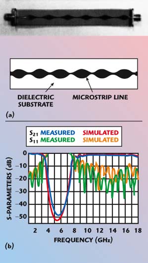
Q. Xue, et al.12 describe a new microstrip transmission line where a PBG structure has been incorporated on the transmission line itself. It consists of a regular 50 Ω line with six periodic perforations. An increased series inductance is obtained from the narrowed lines on both sides of the perforation while an increase of shunt capacitance results from the two edges of the perforation across the width of the microstrip line. Two mirrored triangles are introduced to increase the shunt capacitance and series inductance further and to achieve a tunable cell of the transmission parameters. Two narrow connecting strips connect the triangles to the narrow portions of the microstrip line. The perturbed transmission line and the unit cell are shown in Figure 28. Remarkable additional shunt capacitance is obtained from the gaps between the triangle edges and the end edges of the perforation. The connecting lines and the triangles form a resonant component for enhancing the bandstop phenomena.
 | ||
| Fig. 28 A textured microstrip line with six cells (a), and its unit cell (b). (See Ref. 12, © 1999 IEEE) | ||
The S-parameter’s performance is shown in Figure 29. A stopband between 6.5 to 8.5 GHz is found and the bandwidth of the stopband is more than 25 percent. The phase changes faster at frequencies near the edges of the stopband indicating a slow-wave characteristic. The novel achievement of this structure is the elimination of the dependence of the propagation constant on the orientation and location of the transmission line with respect to the axes of the periodicity of the PBG ground plane.
 | ||
| Fig. 29 S-parameters of a textured transmission line. (See Ref. 12, © 1999 IEEE) | ||
Conclusion
In the first part of this two-part article, the basic PBG configurations and application of PBG structures in enhancing the performance of microwave devices and components have been reviewed. The focus has been on the performance of PBG assisted low noise oscillators, PBG-based microcavities, suppressing the LO leakage in mixers for broadband harmonic tuning, high efficiency power amplifiers, and LPFs and BPFs. The following beneficial points are noted:
- An excellent image guide resonator is achieved by inclusion of PBGs, useful in low noise oscillator design.
- PBG-assisted microcavities provide enhanced spontaneous emission and increase the efficiency of an LED.
- It can be seen that a PBG-based mixer suppresses LO leakage by more than 10 dB.
- An amplifier with perturbed ground plane with PBGs results in intrinsic broadband harmonic suppression without any stub or filtering element. The PAE is also increased.
- In case of LPFs, it can be seen that the PBGs provide more attenuation, complete suppression of spurious transmission without excess conductor loss. The non-uniform PBGs with binomial and Chebyshev distribution provide better performance in terms of ripple height in the passband, selectivity and wider stopband.
- The use of UC-PBGS in a conventional BPF suppresses the second and third harmonics significantly.
- The proposed non-uniform PBGs with binomial distribution is also very useful in suppressing the harmonics in a bandpass filter.
- The packaging issues in implementing PBGs in RF and microwave circuits have also been addressed. Three varieties of PBGs are presented that can alleviate the conventional packaging issues in HMIC and MMIC multilayered configurations.
Thus, the PBG structures find many potential applications in microwave components and devices to enhance their overall performance. In the next part of the article, PBG applications in waveguides, antennas and phased arrays will be presented.
References
- A. Byers, I. Rumsey, Z. Popovic and M.P. May, “Surface-wave Guiding Using Periodic Structures,” IEEE APS-International Symposium Digest, Salt Lake City, UT, Vol. 1, July 17–21, 2000, pp. 342–345.
- D. Sievenpiper and E. Yablonovitch, “Eliminating Surface Currents with Metallodielectric Photonic Crystals,” IEEE International Microwave Symposium Digest, Baltimore, MD, Vol. 2, June 7–12, 1998, pp. 663–666.
- R. Kim and H.Y.D. Yang, “Surface Waves and Leaky Waves in Integrated Circuit Structures with Planar Periodic Dipole Loading,” IEEE APS-International Symposium Digest, Salt Lake City, UT, Vol. 1, July 17–21, 2000, pp. 346–349.
- R. Coccioli and T. Itoh, “Design of Photonic Bandgap Substrates for Surface-Wave Suppression,” IEEE International Microwave Symposium Digest, Baltimore, MD, Vol. 3, June 7–12, 1998, pp. 1259–1262.
- K.P. Ma, J. Kim, F.R. Yang, Y. Qian and T. Itoh, “Leakage Suppression in Stripline Circuits Using a 2-D Photonic Bandgap Lattice,” IEEE International Microwave Symposium Digest, Anaheim, CA, Vol. 1, June 13–19, 1999, pp. 73–76.
- D. Sievenpiper, L. Zhang, R.F.J. Broas, N.G. Alexopolous and E. Yablonovitch, “High Impedance Electromagnetic Surfaces with a Forbidden Frequency Band,” IEEE Transactions on Microwave Theory and Techniques, Vol. 47, No. 11, November 1999, pp. 2059–2074.
- K.C. Chen, C.K.C. Tzuang, Y. Qian and T. Itoh, “Leaky Properties of Microstrip Above a Perforated Ground Plane,” IEEE International Microwave Symposium Digest, Anaheim, CA, Vol. 1, June 13–19, 1999, pp. 69–72.
- V. Radisic, Y. Qian, R. Coccioli and T. Itoh, “Novel 2-D Photonic Bandgap Structures for Microstrip Lines,” IEEE Microwave and Guided Wave Letters, Vol. 8, No. 2, February 1998, pp. 69–71.
- F.R. Yang, Y. Qian, R. Coccioli and T. Itoh, “A Novel Low Loss Slow-wave Microstrip Structure,” IEEE Microwave and Guided Wave Letters, Vol. 8, No. 11, November 1998, pp. 372–374.
- Y. Qian, et al., “Simulation and Experiment of Photonic Bandgap Structures for Microstrip Circuits,” Asia Pacific Microwaves Conference Digest, Hong Kong, December 2–5 1997, pp. 585–588.
- X.Q. Sheng, Edward K.N. Yung and C.H. Chan, “An Efficient Analysis of Microstrip Lines on Artificial Structures,” Asia Pacific Microwaves Conference Digest, Sydney, Australia, December 3–6, 2000.
- Q. Xue, K.M. Shum and C.H. Chan, “Novel 1-D Photonic Bandgap Microstrip Transmission Line,” IEEE APS-International Symposium Digest, Salt Lake City, UT, Vol. 1, July 17–21, 2000, pp. 354–356.
- F.R. Yang, K.P. Ma, Y. Qian and T. Itoh, “A Uniplanar Compact Photonic-bandgap (UC-PBG) Structure and its Applications for Microwave Circuits,” IEEE Transactions on Microwave Theory and Techniques, Vol. 47, No. 8, August 1999, pp. 1509–1514.
- Y. Qian, D. Sievenpiper, V. Radisic, Y. Yablonovitch and T. Itoh, “A Novel Approach for Gain and Bandwidth Enhancement of Patch Antenna,” Radio and Wireless Conference, 1998.
- Y. Qian, R. Coccioli, D. Sievenpiper, V. Radisic, E. Yablonovitch and T. Itoh, “Microstrip Patch Antenna Using Novel Photonic Bandgap Structures,” Microwave Journal, Vol. 42, No. 1, January 1999, pp. 66–76.
- R. Coccioli, F.R. Yang, K.P. Ma and T. Itoh, “Aperture-coupled Patch Antenna on UC-PBG Substrate,” IEEE Transactions on Microwave Theory and Techniques, Vol. 47, No. 11, November 1999, pp. 2123–2130.
- R. Gonzalo, P.D. Maagt and M. Sorolla, “Enhanced Patch Antenna Performance by Suppressing Surface Waves Using Photonic-bandgap Substrates,” IEEE Transactions on Microwave Theory and Techniques, Vol. 47, No. 11, November 1999, pp. 2131–2138.
- E. Yamashita and Y. Qian, “Analysis of Microwave Circuits and Planar Antennas Using the FDTD Method,” Realize Inc., Tokyo, Japan, May 1996.
- K.M. Shum, Q. Xue, C.H. Chan and K.M. Luck, “Investigation of Microstrip Reflectarry Using a Photonic Bandgap Structure,” Microwave and Optical Technology Letters, Vol. 28, No. 2, January 20, 2001, pp. 114–116.
- P.S. Hui and A. Alphones, “Microstrip Patch Antenna with Annular Ring PBG,” Asia Pacific Microwave Conference 2000, Sydney, Australia, December 2000, pp. 1347–1351.
- R. Gonzalo, B. Martinez, P.D. Maagt and M. Sorolla, “Patch Antennas on Photonic Crystal Structures,” http://www.ecs.umass.edu/ece/allerton/99/34/.
- Y. Qian, R. Coccioli, F.R. Yang and T. Itoh, “Passive and Active Component Design Using PBG,” IEEE Sixth International Conference on Terahertz Electronics Proceedings, 1998, pp. 42–45.
- R. Coccioli, M. Boroditsky, K.W. Kim, Y. Rahmat-Sami and Y. Yablonovitch, “What is the Smallest Possible Electromagnetic Mode Volume in a Dielectric Cavity?,” IEE Proceedings, 1998, pp. 42–45.
- N.C. Karmakar and M.N. Mollah, “Microstrip Lines on Annular Ring Photonic Bandgap Structures,” Microwave and Optical Technology Letters, Vol. 32, No. 6, March 20, 2002, pp. 431–433.
- F.R. Yang, Y. Qian and T. Itoh, “A Novel Uniplanar Compact PBG Structure for Filter and Mixer Applications,” IEEE International Microwave Symposium Digest, Anaheim, CA, Vol. 3, June 13–19, 1999, pp. 919–922.
- Y. Qian, F.R. Yang and T. Itoh, “Characteristics of Microstrip Lines on a Uniplanar Compact PBG Ground Plane,” Asia-Pacific Microwave Conference Digest, Yokahama, Japan, December 8-11, 1998, pp. 589-592.
- E.R. Brown, C.D. Parker and E. Yablonovitch, “Radiation Properties of a Planar Antenna on a Photonic-crystal Substrate,” Journal of the Optical Society of America, B. Optical Physics, Vol. 10, No. 2, February 1993, pp. 404–407.
- A. Harvey, “ Periodic and Guiding Structures at Microwave Frequencies,” IRE Transactions on Microwave Theory and Techniques, Vol. 8, June 1959, pp. 30–61.
- 29. D. Nesic and A. Nesic, “Bandstop Microstrip PBG Filter with Sinusoidal Variation of the Characteristic Impedance and Without Etching in the Ground Plane,” Microwave and Optical Technology Letters, Vol. 29, No. 6, June 20, 2001.
- S.K. Sharma and L. Shafai, “Enhanced Performance of an Aperture-coupled Rectangular Microstrip Antenna on a Simplified Unipolar Compact Photonic Bandgap (UC-PBG) Structure,” IEEE-APS International Symposium Digest, Boston, MA, July 8–13, 2001, pp. 498–501.
- 31. N.C. Karmakar and M.N. Mollah, “Investigation into Non-uniform Photonic Bandgap Microstripline Low Pass Filters,” IEEE Transactions on Microwave Theory and Techniques, Vol. 51, No. 2, February 2003, pp. 564–572.
- 32. V. Radisic, et al., “Novel Architectures for High Efficiency Amplifiers for Wireless Applications,” IEEE Transactions on Microwave Theory and Techniques, Vol. 46, No. 11, November 1998, pp. 1901–1909.
- 33. C.Y. Hang, W.R. Deal, Y. Qian and T. Itoh, “High Efficiency Transmitter Front-ends Integrated with Planar Antennas and PBG,” 2000 Asia-Pacific Microwave Conference, Australia.
- 34. D.M. Pozar, Microwave Engineering, Addison-Wesley, Reading, MA, 1990.
- 35. N.C. Karmakar, “Theoretical Investigations into Binomial Distributions of Photonic Bandgaps on Microstripline Structures,” Microwave and Optical Technology Letters, Vol. 33, No. 3, May 5, 2002, pp. 191–196.
- 36. N.C. Karmakar, “Improved Performance of Photonic Bandgap Microstripline Structures Using Chebyshev Distribution,” Microwave and Optical Technology Letters, Vol. 33, No. 1, April 5, 2002, pp. 1–5.
- 37. N.C. Karmakar and M.N. Mollah, “Harmonic Suppression of a Bandpass Filter Using Binomially Distributed Photonic Bandgap Structures,” IEEE-APS International Symposium Digest, Columbus, OH, July 22–27, 2003, pp. 883–886.
- 38. T. Akaline, M.A.G. Laso, T. Lopetgi and O. Vanbesien, “PBG-type Microstrip Filters with One-end and Two-sided Patterns,” Microwave and Optical Technology Letters, Vol. 30, No.1, July 5, 2001.
 Nemai Karmakar obtained his B.Sc. (EEE) and M.Sc. (EEE) degrees from Bangladesh University of Engineering and Technology, Dhaka, Bangladesh, in 1987 and 1989 respectively, his M.Sc. degree in electrical engineering from the University of Saskatchewan, Saskatoon, Canada, in 1991, and his PhD degree from the University of Queensland, Brisbane, Australia, in 1999. He worked as an assistant engineer at the Electronics Institute, Atomic Energy Research Establishment, Dhaka, between 1989 and 1990. In August 1990 he served as a research assistant at the Communications Research Group, University of Saskatchewan. From 1992 to 1995 he worked as a microwave design engineer at Mitec Ltd., Brisbane, where he contributed to the development of land mobile satellite antennas for the Australian Mobilesat™. From 1995 to 1996 he taught final year courses on microwaves and antenna technologies at Queensland University of Technology, Brisbane. From September 1998 to March 1999 he worked as a research engineer at the Radar Laboratory, Nanyang Technological University, Singapore. He is currently an assistant professor and graduate advisor in the division of communications, the school of electrical and electronic engineering, Nanyang Technological University. His research interests include broadband microstrip antennas and arrays, beam-forming networks, smart antennas, near-field/far-field antenna measurements, microwave device modeling, monostatic and bistatic radars. He has published more than 100 journal and conference papers, and three book chapters.
 Mohammad Nurunnabi Mollah obtained his B.Sc. degree in electrical and electronic engineering from Rajshahi University of Engineering and Technology (RUET), Bangladesh, in 1986, and his M.Sc. degree in electrical and electronic engineering from Bangladesh University of Engineering and Technology (BUET), Dhaka, Bangladesh, in 1987. He is currently working towards his PhD degree in the communication engineering division of Nanyang Technological University (NTU), Singapore. His doctoral degree concerns PBG assisted reconfigurable phased array antennas. In 1990 he joined the department of electrical and electronic engineering of KUET as a lecturer; he became an assistant professor in 1993 and associate professor in 1998. He has authored or coauthored 32 papers in referred journals and conferences. His research interests include microstrip patch antennas and arrays, microwave passive devices, and electromagnetic bandgap structures. He is a Fellow of the Institution of Engineers Bangladesh (IEB) and a student member of IEEE.