W-CDMA is one of the most important requirements of 3G mobile communication systems,1 and it presents a challenge to the design of RF systems for W-CDMA mobile terminals. Compared with a conventional superheterodyne structure, the direct RF I/Q modulation shows the advantages of a simple circuit configuration and low cost, although it is difficult to build a direct conversion transceiver with good performance, especially a direct conversion receiver. A new transceiver structure2,3 is shown in Figure 1, which is a combination of a superheterodyne receiver and a direct modulation transmitter. To support that approach, a special dual loop PLL is developed, which serves as local oscillators at 1920 to 1980 MHz and 380 MHz, the two local oscillator frequencies that support the frequency bands (Rx: 2110 to 2170 MHz; Tx: 1920 to 1980 MHz) according to third-generation partnership project (3GPP) protocol.4
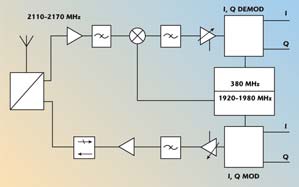
Fig. 1 A combined transceiver structure.
PLL Design and Simulation
The dual PLL module includes two frequency synthesizers. The RF PLL’s frequency range is 1920 to 1980 MHz with a 200 kHz frequency raster. The IF PLL operates at 380 MHz.
A typical phase model of a phase-locked loop is shown in Figure 2, where Kp is the phase gain of the phase detector, Z(S) is the transfer function of the loop filter and Kvco is the voltage control sensitivity of VCO.
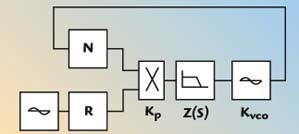
Fig. 2 Phase model of a phase-locked loop.
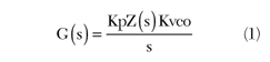
The open loop transfer function is given by
The stop band of the loop, ωc, can be defined when

The common factor of the closed loop transfer function for the R and N dividers and the phase detector can be simplified into two cases
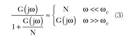
The closed loop transfer function of the VCO can be simplified in two cases
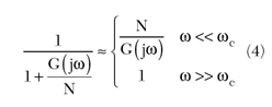
Comparing Equations 3 and 4, it can be seen that the noise of the divider and phase detector dominate the close-in phase noise, and the VCO noise dominates the out-of-band phase noise.
Although the N divider, R divider, phase detector and reference frequency contribute to the close-in phase noise, the phase detector plays the most important role. To estimate the close-in phase noise, the data sheet of the PLL chip gives the phase noise floor of phase detector normalized to 1 Hz (P1Hz), and the formula used is
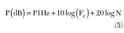
where
Fc = reference frequency
To lower the close-in phase noise, a higher frequency can be selected. Accordingly, a fractional-N PLL is a better choice.5
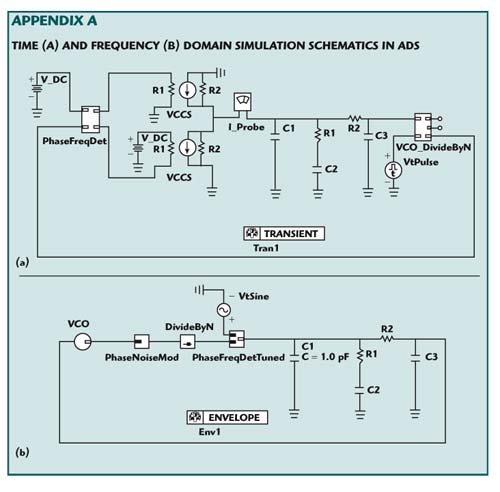
A platform was built in Agilent ADS to simulate the performance of PLLs including locking time and phase noise. Two schematics were drawn to support simulations in both the time and frequency domains. This simulation process provides a very important measure to evaluate the PLL structure and the parameters of key components. When the structure and parameters have been selected and laid on a PCB, it will be a time-consuming job to change it. The two schematics are shown in Appendix A.
In ADS, a method called envelope simulation is adopted to perform complex signal analysis.6,7 It combines features of time- and frequency-domain representation. This simulator permits input waveforms to be represented in the frequency domain as RF carriers, with modulation “envelopes” that are represented in the time domain

Each time-varying spectrum, Vk(t), can be thought of as a modulation waveform (envelope) with a center frequency k. This spectrum may represent transient signals with continuous spectra or periodic signals with discrete spectral lines. Compared with the conventional time-domain method, envelope only focuses on the varying of the envelopes, which varies much slower than the carrier, and will make the simulations much faster. Figure 3 shows the typical simulation results of the PLL.

Fig. 3 Time (a) and frequency (b) domain simulation results.
RF VCO Design and simulation
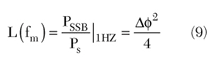
The phase noise is the key feature of an oscillator. Normally, the phase noise is characterized by L(fm) = PSSB/PS|1Hz, the ratio of the power at a frequency offset within 1 Hz to the total carrier power. The following will show why this power ratio can characterize the phase noise.8 A phase modulated signal as
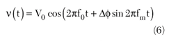
can be series expanded to
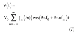
where
Jn = Bessel function
When Δφ is small enough
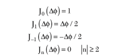
Then Equation 7 can be simplified to

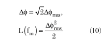
Thus, the relationship between L(fm) and Δφ is
To estimate the phase noise performance, an oscillator can be thought as a phase feedback system, as shown in Figure 4, where Δθ(ωm) is the input phase variation, Δφ(ωm) is the output phase variation and L(jωm) is the equality transfer function of the resonant tank.

Fig. 4 Phase model of an oscillator.
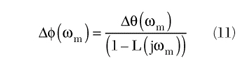
The system transfer function is
![]()
Rewritten, it becomes
For a normal LC resonance tank
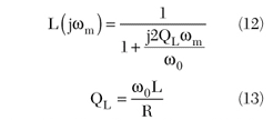
Inserting Equations 12 and 13 into Equation 11 and expressing it in power density yields

Where the thermal noise of the amplifier is

This is Leeson’s equation.7,9
According to Equations 14 and 15, a higher QL will help to get better phase noise performance, although a tradeoff must be made between good performance and compact size because of the size limit of a mobile terminal. After many simulations, fabrication and test, a special circuit structure was selected to meet the performance and size requirement. That circuit includes both lumped components and distributed components. The key component that affects phase noise most significantly is the resonant circuit, especially the inductor (lumped inductors working at high frequency always have low Q factors). A Clapp circuit structure and a distributed inductor were selected to improve the Q factor. The difference between a Colpitts and a Clapp topology is C3. This series capacitor affects the resonance frequency and works as a DC block. The schematics in ADS are shown in Figure 5.

Fig. 5 Oscillator topology (a) and ADS schematic of the RF VCO (b).
The simulation results of S-parameter and transient analysis in ADS are shown in Figure 6; Figure 7 shows the simulation results of harmonic balance.

Fig. 6 S-parameter (a) and transient (b) simulation results.

Fig. 7 Simulated phase noise (a) and harmonic suppression (b).
Fabrication and Test
After the simulations of the module, fabrication can be started. To improve the pulling parameter of the RF VCO and the isolation between VCO and transceiver, an integrated dual output amplifier (MAX2472) is inserted as a VCO buffer. The IF VCO is based on a fully integrated dual output oscillator chip (MAX2620), which has the same circuit structure. All lumped components are in 0603 or 0402 packages, and the whole module is laid on a 25 by 32 mm FR4 PCB board. The test result of the module shows good performance — the phase noise of the PLL at 1.9 GHz is better than –84 dBc/Hz at 10 kHz offset; the phase noise of the PLL at 380 MHz is better than –92 dBc/Hz at 10 kHz. Figures 8 and 9 show the PCB layout and a typical RF output spectrum.

Fig. 8 PCB layout.

Fig. 9 Typical RF output spectrum.
Conclusion
This special PLL module was embedded into a W-CDMA mobile terminal to act as the local oscillators. The RF specifications of a W-CDMA mobile terminal were measured. The output power reached 23 dBm, and the minimum received level was less than –110 dBm. The EVM of the transmitter was less than 15 percent. Figure 10 shows the transmitter EVM test and the output I,Q waveform of the receiver; Figure 11 shows the Rx EVM test result with adjacent channel selectivity (ACS). The RF specifications meet the requirement of 3GPP standard.

Fig. 10 Transmitter EVM test results (a) and receiver I, Q outputs (b).

Fig. 11 Receiver EVM test with adjacent channel selectivity (ACS).
References
- X. You, “Development of the 3rd Generation Mobile Communication,” Electronic Journal, No. 11A, 1999.
- J. Liu, “W-CDMA RF Module Design with Direct Modulation,” Asia-Pacific Microwave Conference.
- W. Jiang, “A Special, Compact PLL Module Fits W-CDMA MT,” Asia-Pacific Microwave Conference.
- 3GPP TS 25.103, RF Parameters in Support of Radio Resource Management, http://www.3gpp.org.
- http://www.national.com/appinfo/wireless/files/DeansBook_4_01.pdf, National Semiconductor.
- H.S. Yap, “Designing to Digital Wireless Specifications Using Circuits Envelopes Simulation,” HP EEsof Division.
- Advanced Design System online manual, Agilent Technology.
- J. Bai, Low Noise Frequency Synthesizing, Xi’an JiaoTong University Publishing House, 1995.
- D.B. Leeson, “A Simplified Model of Feedback Oscillator Noise Spectrum,” Proceedings of the IEEE, Vol. 42, February 1965.
-