
Due to the growing demand for broadband wireless communications, the operating frequency is moving toward the 5 GHz U-NII band. The advantage of combining the baseband circuitry and the RF front-end on one single chip for cost savings is strongly desired for highly integrated system-on-chip (SoC) applications. Due to speed improvements, the unity gain frequency fT of a CMOS device, fabricated by a standard process, has become comparable to that obtained with a GaAs process. Recently, many RF circuits have been realized with the CMOS process. The requirements of low power and low cost have pushed the trend toward a single radio chip.1 This article presents a 5.7 GHz differential CMOS LNA and a Gilbert-cell mixer for 802.11a WLAN applications, as shown in Figure 1. The output of the differential CMOS LNA is connected to a balun and passes through an image rejection filter to the single-ended mixer. The LNA and mixer are fabricated with a TSMC 0.18 mm standard CMOS process. The layout of the fabricated LNA/mixer RFIC is also shown. The die size is 0.9 × 2.0 mm.

Fig. 1 A 5.7 GHz CMOS differential LNA and Gilbert-cell mixer in a WLAN receiver front-end; (a) its schematic and (b) the layout of the LNA/mixer RFIC.
CMOS Differential LNA
Figure 2 shows the circuit schematic of the 5.7 GHz CMOS differential LNA with current reuse. The LNA is made insensitive to off-chip components because of the virtual ground characteristic of the differential topology and is saving power through the current-reused topology.2 The cascode amplifiers, M1 and M2, share the same quiescent current with the next common source amplifier M3, which means the LNA has the linear gain of a two-stage amplifier and the power consumption of one stage. The bypass capacitance Cbypass achieves the common source configuration of the second-stage amplifier. Lb1 to Lb5 are the bondwire equivalent inductances.

Fig. 2 The 5.7 GHz CMOS differential LNA with current reuse; (a) schematic and (b) test board.
Input, Output and Inter-stage Matching
Shaeffer and Lee3 define the sources of noise and show how to determine the gate width of the first-stage transistor. Under a given power consumption limit, the optimum gate width occurs when the drain-current noise and the induced-gate noise, referred to the same node, are comparable. The chosen gate width of the first-stage transistor M1 is 160 µm. A multi-finger layout technology is used to reduce the noise of the transistor gate resistance. To achieve an input matching to the 50 Ω characteristic impedance of the system, the series connection of the equivalent bondwire inductance Lb2, the capacitance C1 and the equivalent bondwire inductance Lb1 of the source-degeneration is used. The equivalent bondwire inductance Lb1 is used to match the real part of the input impedance to the 50 Ω characteristic impedance. The combination of the gate and source bondwire equivalent inductances cancels the reactance of the capacitance Cgs (at the resonant frequency ωo) of the input transistor M1. The input impedance Zin is given by3

When at the resonant frequency

where

The on-chip inductance L1 is used as the first-stage inductive load. To realize an RF choke, let the inductor L1 and the equivalent parallel capacitance at a node A resonate at a frequency close to the operating frequency range, which is the same as conjugate matching between two-stage amplifiers. The conjugate matching at high impedance provides high gain and compresses the noise contribution of the latter stage considerably. However, it does not mean that the higher the impedance, the better the performance, because attention should also be paid to the bandwidth and the circuit stability. Conjugate matching at very high impedance may lead to too narrow a bandwidth and potential instability. There is a tradeoff between gain, noise figure, bandwidth and stability. For the second-stage amplifier, M3, the parallel resonant frequency of the bondwire equivalent inductance Lb3 and the capacitance C4 is designed to be close to the operating frequency. The capacitance C5 and the equivalent inductance bondwire Lb5 in series performs the output matching to the characteristic impedance of the system.
Simulation and Measured Results
The LNA measurements were performed on a FR-4 PCB test fixture. The LNA chip is connected to the test board with aluminum bondwires. The effects of the bondwires and the FR-4 test board are all taken into account in the simulations. Note that there are two 5.7 GHz microstrip 180° hybrid ring couplers connected to the differential input and output ports of the LNA. This is to generate and combine a differential signal for measurement. The return loss of the ring coupler is higher than 20 dB and its insertion loss is approximately 1 dB at 5.7 GHz. The effect of the ring coupler has been taken into account in both simulation and measurement de-embedding. The simulated and measured gain and the input return loss measured at 5.775 GHz are 20.4/8 dB (2 dB should be added for the two rat race ring losses) and –21/–22 dB, respectively, as shown in Figure 3. The simulated and measured isolation and output return loss are –38/–20 dB and –19/–32 dB, respectively. Table 1 summarizes the measured performance of the designed 5.7 GHz LNA (after de-embedding the input and output ring coupler).
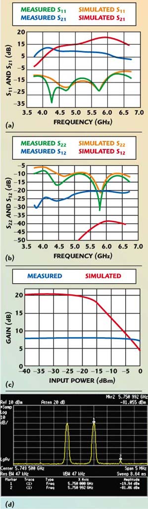
Fig. 3 Simulated and measured performance of a 5.7 GHz CMOS differential LNA; (a) gain and input return loss, (b) isolation and output return loss, (c) input P1dB and (d) two-tone test.
CMOS Single-ended Mixer
As shown in the diagram of the 5.7 GHz WLAN receiver front-end, a Gilbert-cell type mixer is connected to the filters. The mixer comprises an input transconductance stage and two differential switching pairs. The transconductance amplifier M1 transfers the received RF signal into a current format. The switching pairs M2 and M3 (controlled by the LO) then perform the mixing operation, down-converting the RF signal into the IF. Compared with a single-balanced mixer, the advantages of the Gilbert-cell type mixer include increased linearity, higher common mode rejection ratio (CMRR) and a lower LO signal at the output, which avoids saturating the next stage. The cost of the good LO-IF isolation of the Gilbert-cell type mixer is a higher noise figure than for a single balanced mixer for the same power consumption. Nevertheless, considering the merits of a Gilbert-cell type mixer, including linearity and CMRR, and that the effect of the higher noise figure of the mixer on the entire system will be compressed by the gain of LNA, cost is not a very serious issue.
Circuit Design
The transcondutance, noise figure and linearity of the mixer are mostly governed by the M1 device. Considering the power consumption and the parameters mentioned earlier, the widths of M1 were chosen to be 160 µm. The transistors M2 and M3 are acting like two switching pairs, and the switching ability is the most important concern when deciding the width of these transistors. A larger transistor width implies that the loss of the switch could be lower. However, this will result in a higher parasitic capacitance at node B. The RF signal will be attenuated by these capacitors and the noise figure of the mixer will be increased.
The circuit schematic of the mixer and the FR-4 PCB test board are shown in Figure 4. The output signals are combined by a current mirror and delivered to the output buffer. Using the current mirror as an active load will not only provide high gain at the IF but also eases the output matching and measurement (only one port needs to be considered). For saving power consumption and to avoid attenuating the signal too much, a common source transistor is used as a buffer instead of a source follower.4 To present an output impedance as small as 50 Ω, a source follower with a very large gm must consume a large current. Even if a 50 Ω output impedance is achievable, the signal voltage at the source is half of that at the gate of the source follower, which reduces the signal power by approximately 6 dB. On the contrary, if a common source transistor is used as a buffer, the load of the transistor presents a 50 Ω output impedance with a voltage gain (the product of gm and the load at the drain of M6). It will not only reduce the power consumption (since there is no need for a large current) but will also provide gain. The LO input matching uses on-chip components and the RF and IF output matching uses off-chip components.
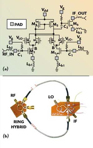
Fig. 4 A 5.7 GHz CMOS single-balanced mixer; (a) schematic and (b) FR-4 PCB test board.
Simulation and Measurement
Using a 180° hybrid power divider connected to an RF signal generator provides the differential LO for measurement. The mixer dissipates 15 mW from a 2.5 V supply. The simulated and measured results are shown in Figure 5. With an RF varying from 5.725 to 5.825 GHz and an IF at 480 MHz, the measured conversion gain is 8 dB, the input P1dB is 0 dBm, the IIP3 is 1.57 dBm, the noise figure is 14 dB, the LO-RF isolation is 28 dB and the LO-IF isolation is 35 dB. Table 2 summarizes the measured performance of the mixer.

Fig. 5 Simulated and measured performance of a 5.7 GHz CMOS Gilbert-cell mixer; (a) input return loss, (b) IF output return loss, (c) conversion gain and input P1dB, (d) two-tone test and (e) noise figure (DSB).

RF Front-end Integrated Measurement
Figure 6 shows the block diagram and photograph of an integrated 5.7 GHz receiving RF front-end for performance measurement. A discrete GaAs FET LNA is used between the RF band-select filter and the CMOS LNA/mixer RFIC to increase the conversion gain. Table 3 depicts the measured characteristics of each stage and the integrated RF front-end. Figure 7 shows the measured performance. The RF front-end exhibits a conversion gain of 16 dB, a noise figure of 6.3 dB, an input P1dB of –21 dBm and an input IP3 of –11.7 dBm. The image rejection ratio is about 60 dB. Table 4 depicts the demodulated error vector magnitude (EVM) of the IEEE 802.11a WLAN OFDM measurement. The measured EVM for the 802.11a 54 Mbps OFDM test (64-QAM) is 1.43 percent.

Fig. 6 An integrated 5.7 GHz receiving RF front-end (a) and its block diagram (b) .


Fig. 7 Measured performance of an integrated 5.7 GHz RF front end; (a) conversion gain and P1dB, (b) noise figure, (c) two-tone test and (d) 802.11a 54 Mbps OFDM test.

Conclusion
A 5.7 GHz CMOS differential LNA and a Gilbert-cell CMOS mixer using a 0.25 mm CMOS technology for 802.11a WLAN applications are presented. The CMOS differential LNA uses a current-reuse technology to increase the linear gain and reduce power consumption. The differential LNA measurements at 5.775 GHz exhibit a noise figure of 5.8 dB, a linear gain of 10 dB, P1dB of 0 dBm, with a power consumption of 30 mW at 2.5 V. The change in gain of the LNA may be attributed to the change in resonant frequency of the LC tank at node A. The output signals of the mixer are combined by current mirror and delivered to a 50 Ω load through a common source buffer. The measured conversion gain is 8 dB, the input P1dB is –3 dBm and the noise figure is 14 dB, the LO-RF isolation is 28 dB and the LO-IF isolation is 35 dB. The power consumption of the mixer is 15 mW at 2.5 V. A discrete GaAs FET LNA is used between the RF band-select filter and the CMOS LNA/mixer RFIC for the performance measurement of the integrated receiving RF front-end. The RF front-end exhibits a conversion gain of 16 dB, a noise figure of 6.3 dB, an input P1dB of –21 dBm and an input IP3 of –11.7 dBm. The measured image rejection ratio is approximately 60 dB. The measured EVM for the 802.11a 54 Mbps OFDM test (64-QAM) is 1.43 percent. n
Acknowledgment
The authors would like to thank the Chip Implementation Center (CIC) of the National Science Council, Taiwan, ROC, for supporting the TSMC CMOS process.
References
- T.H. Lee, The Design of CMOS Radio-frequency Integrated Circuits, Cambridge University Press, New York, NY, 1998.
- B. Razavi, Design of Analog CMOS Integrated Circuits, McGraw Hill, New York, NY, 1996.
- D.K. Shaeffer and T.H. Lee, “A 1.5 V 1.5 GHz CMOS Low Noise Amplifier,” IEEE Journal of Solid-State Circuits, Vol. 32, No. 5, May 1997, pp. 745–759.
- H. Samavati, H.R. Rategh and T.H. Lee, “A 5 GHz CMOS Wireless LAN Receiver Front-end,” IEEE Journal of Solid-state Circuits, Vol. 35, No. 5, May 2000, pp. 765–772.