Over the past two decades, the military market has widely embraced the use of monolithic microwave integrated circuits (MMIC). The MMIC Program of the mid-1980s brought about significant advances in the design, manufacture and test capability of GaAs MMIC components. The advantages of using MMICs over their MIC/discrete hybrid counterparts include lower total cost, easier assembly and more consistent performance, and the impact of these advantages increases with the frequency of operation. Components used in today’s military systems must exhibit very high performance, and be robust enough to operate in harsh land-, sea- and air-based environments. While a discrete solution generally provides the fewest sacrifices in electrical performance, achieving consistent results in volume production at Ka-band, without the use of MMICs, can be challenging.

While MMIC components and subsystems find use across the microwave and millimeter-wave spectrum, the Ka-band, and in particular the 29 to 36 GHz band, is home to many important applications for MMIC components. A relative null in the RF absorption of the atmosphere near the middle of this band drives the use of many military electronic warfare (EW) applications including radar, missile seekers and target acquisition. This same feature is also useful for other applications such as military/satellite communications, radio astronomy, radio navigation and of course the terrestrial point-to-point microwave radio band from 31.8 to 33.4 GHz. While it can be less expensive to build communications systems at lower frequencies, the shorter wavelengths associated with the millimeter-wave bands offers several system level advantages, including smaller antennas for a given beam width and more accurate target acquisition capabilities.
In order to address these applications specifically, Hittite Microwave has released the HMC566 GaAs pHEMT (pseudomorphic high electron mobility transistor) MMIC low noise amplifier (LNA). The HMC566 is a wide band LNA chip that is specified from 29 to 36 GHz. The device employs a four-stage single-ended topology where the first two input stages of the amplifier are optimized for lowest noise figure, while the output stage is matched to provide broad, flat output P1dB and output IP3 characteristics. Each of the four stages is independently self-biased. Bond pads for all drain bias lines (Vdd1, Vdd2, Vdd3 and Vdd4) are presented on one side of the chip, and only a few bias decoupling capacitors are required to achieve unconditional stability. The HMC566 also features on-chip DC blocks on the RF input and output, and the amplifier is suitable for either epoxy or eutectic die attach.
The HMC566 LNA provides 20 dB of small-signal gain and 2.8 dB of noise figure at mid-band (see Figure 1). The LNA also provides a positive gain slope across the operating band, which will be especially welcome in subsystem applications where the amplifier is operated over a wider band. This feature serves to counteract the inherent insertion loss roll-off versus frequency exhibited by microwave and millimeter-wave printed circuit substrates and interconnects. The small-signal gain level is generally monotonic versus temperature allowing for straightforward temperature compensation if required at the system level. The noise figure performance of the HMC566 is well behaved and generally increases by 1 dB or less from +25° to +85°C.
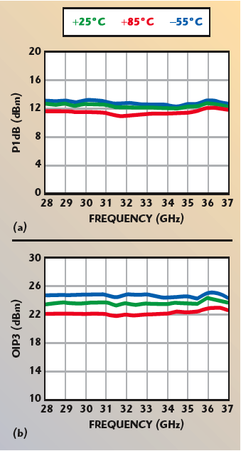
Another significant feature of the HMC566 amplifier is its single voltage supply operation. The device is self-biased and operates from a single +3 V supply, consuming only 60 mA. The linearity of this LNA is very consistent across its rated band, with output P1dB and the output IP3 performance of +12 and +24 dBm, respectively (see Figure 2). Such performance enables the HMC566 to be used in various applications, including low noise, LO buffer and transmit gain block applications. Since the typical P1dB and IP3 values vary by less than 3 dB from –55° to +85°C, the designer does not have to overdesign the linearity of the RF chain, potentially driving up DC power consumption, in order to meet system level specifications at the operating temperature extremes.
The HMC566 LNA is ideal for hybrid and multi-chip module (MCM) assembly applications due to its compact size, convenient layout and flexible mounting options. It is fabricated in a mature GaAs pHEMT process. This volume production fabrication process has been qualified by Hittite for use in various military and space programs.

Whether discrete or MMIC, the GaAs pHEMT device is the workhorse of the low noise receiver chain. Transceiver designers know that millimeter-wave LNAs fabricated in a sub-micron geometry GaAs pHEMT process can deliver low noise figure, high gain and high efficiency. The simplified block diagram, shown in Figure 3, is an example of how the HMC566 GaAs pHEMT MMIC LNA may be combined with other Hittite components to construct a Ka-band receiver and LO generation chain. The company offers an extensive line of VCOs, mixers, dividers, multipliers and amplifiers, which are suitable for applications in this frequency range. This entire block diagram can be constructed without a negative voltage supply since all of these components are either passive, or operate from +3 or +5 V.
The HMC566 GaAs pHEMT MMIC LNA die and each of the products shown in the block diagram are available from stock and can be ordered via the company’s e-commerce site or via direct purchase order. Released data sheets and S-parameter data are available on-line at www.hittite.com. The HMC566 GaAs pHEMT MMIC LNA will also be available in a RoHS-compliant, 4x4 mm surface-mount compatible package in late 2006.
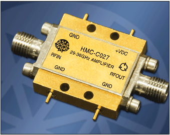
The HMC-C027, shown in Figure 4, is a 29 to 36 GHz low noise amplifier module and is intended for applications where a hermetic packaged module format is required. The HMC-C027 module incorporates the HMC566 and additional features not found in the die version, such as bias decoupling, over-voltage and ESD protection circuitry for added robustness. The hermetic module package also features field-replaceable 2.92 mm connectors, which are essential in test equipment and laboratory settings where numerous connector mating and unmating cycles may be required.
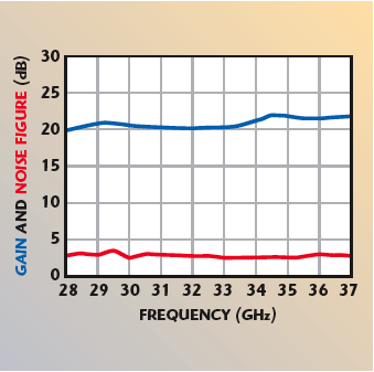
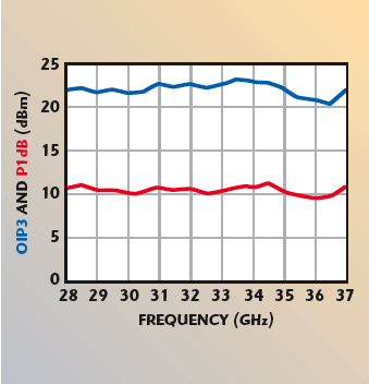
The small-signal and noise figure performance of the HMC-C027 is similar to the bare die version. Figure 5 shows the small-signal gain and noise figure performance of the HMC-C027 versus frequency. As in the die version, the HMC-C027 exhibits a slightly positive gain slope, and a low, flat noise figure. As shown in Figure 6, the linearity performance of the HMC-C027 is only slightly lower than the die version, exhibiting output P1dB and IP3 values of +10 and +22 dBm, respectively.
The HMC-C027 is unconditionally stable, and is rated for operation from –55° to +85°C. As with Hittite’s other module products, the HMC-C027 is available from stock and can be assembled and screened for military and space applications. Released data sheets and S-parameter data are available on-line.
Hittite Microwave Corp.,
Chelmsford, MA
(978) 250-3343,
www.hittite.com.