
The power amplifier in telecommunication is one of the oldest pieces of the transmission system and has continuously evolved over the years. Over the past decade, RF power amplifier design has witnessed tremendous improvement with the advent of window-based computer-aided design, allowing engineers to do real-time modeling and load-pull measurements before even lifting a soldering iron. In addition, manual and cumbersome test equipment that could only do basic modulation has given way to sophisticated test equipment that allows us to create complex digital signals and make measurements in seconds.
The days of fickle transistors with limited power handling and low frequency response are no more. Better power devices and gain blocks are available and continue to improve each year with regard to linearity and efficiency. Today’s new power devices include:
-
GaAsFET devices that have better power linearity and the comfort of operating at elevated temperature.
-
LDMOS devices that provide lots of power and efficiency without running into complex circuitry to achieve high output power.
-
MMICs that not only provide higher power and gain but also serve as RF power pull down and gain controls.
-
GaN (gallium nitride) and SiC (silicon carbide) devices, all promising happy days for power amplifier designers.

Every component that is involved in the making of power amplifiers has seen a dramatic improvement in quality and functionality.
With all these advancements in power device technology one can imagine that designing a “good” power amplifier should be easy. In some ways that is true, but in many others it is not.
The growth in communication technology brings with it a more stringent demand on power amplifier design engineers to come up with amplifiers that can handle analog and digital modulated signals with little or no distortion, higher efficiency and offer many different interface/communication protocols. Yes, there are engineering tools available to help meet these challenges but the complexity of the new modulation modes, demands for ultra high linearity and differing interface control systems have taken the task to a new level. An engineer with specific experience in wireless power amplifier design is an absolute must, as these designs are no longer “kitchen table projects.”
As an example, this article will examine a WiMAX orthogonal frequency division modulation (OFDM) amplifier. This is a standard (IEEE 802.16)-based wireless technology that promises broadband connectivity and can be deployed for various applications. This power amplifier (PA), like in any base station, is usually the most expensive module in the system and the one most likely to diminish the mean time between failure (MTBF) of the base station, so the issue of quality and reliability has to be addressed from the design conception of the PA.
The power amplifier design engineer must understand the system requirements of the amplifier and the IEEE 802.16 requirements effect on the amplifier:
-
What is the downlink power need?
-
What is the peak-to-average power ratio of IEEE 802.16 OFDM signal?

-
What parameters effect the error vector magnitude (EVM)/(RCE) relative constellation error characteristics of the power amplifier?
-
The environment that the PA will be operating within is very important as it will influence the choice of power devices, taking into consideration the junction resistance, channel temperature, drain efficiency, along with the mechanical structure and heat sinking.

A New PA Design
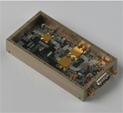
In designing the AR Modular RF 20 W model KMS1070 WiMAX amplifier, Eudyna (formally Fijitsu) GaAsFETs and Hittite devices were chosen considering the power supply requirements and the hostile environment the PA must operate in. The block diagram in Figure 1 illustrates the basic building block of the KMS1070 PA module.
In addition, quality factors were taken into consideration since this module is likely to be produced in thousands, so no technician tweaking will be needed after the board has gone through an automated assembly line. The circuit topology using a balanced configuration was chosen to enhance repeatability and also to take into account the wide band requirement of the PA. Signal reflections due to mismatches caused by component discrepancies that normally degrade digital signal performance will be canceled out using this arrangement. A small-signal simulation was done to optimize gain and stability of the amplifier. The driver stages are perfectly matched I/O power devices that will further reduce the need for tuning the cascade sections in production.
Sparing the mathematical and simulation details of this WiMAX power amplifier design, which, of course, is not any different from any other digitally modulated signal power amplifier, there are some pertinent issues that are vital to achieve a better EVM number in a WiMAX power amplifier.
One of the key issues is the physical location of the DC insertion points to the gate and drain of the power devices. This has a big effect on the RCE number and the quality of the output signal. Phase and amplitude mismatches are also an issue to watch for.
Separating the RF and DC bias voltage ground at the drain of the FET is a good practice which will diminish the chances of the power amplifier going into oscillation because of the large signal envelope swing and the high peak-to-average power ratio of the WiMAX-OFDM signal with approximately 200 sub-carriers.
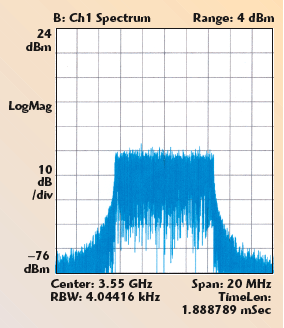
The Agilent E4440A PSA spectrum analyzer and the 89600 vector signal analysis software were used to verify the design. The results in Figure 2 show the spectral quality of the KMS1070 at 3 W output power of a WiMAX (IEEE 802.16) signal.
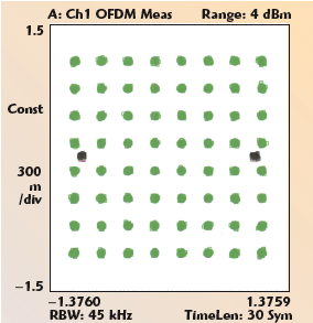
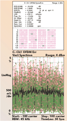
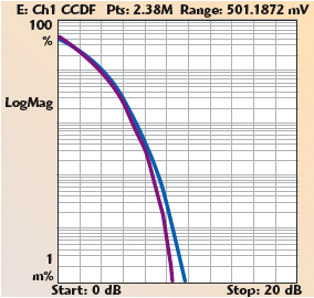
The OFDM subframe information in Figure 3 shows the details of the modulation format used, while Figure 4 shows graphic results, indicating how tightly guarded the I/Q and the tabular function is (shown in Figure 5). These data verify that the module has an impressive 1.9 percent EVM across the frequency band of 3.4 to 3.7 GHz. The complementary cumulative distribution function (CCDF) curve (see Figure 6) shows the peak-to-average power deviation is below the Gaussian noise reference line with little power waste. It should be noted that there is no change in the quality of the signal when the bandwidth is increased from 10 to 20 MHz.
The gain-frequency response has to be extremely stable across the entire operating frequency band and a temperature range of 0° to 60°C. Figure 7 shows a ±0.25 dB result. This number was maintained at all temperatures.
Packaging and Layout
The housing of an amplifier such as this unit is an important part of the design. It is important to try and contain the RF fields and RF ground currents within the RF amplifier portions of the housing. Ideally, if room exists, the RF and control systems should be separated by some physical distance, or contained within a walled structure or box. Secondary components on the ground side of the board should be avoided if possible as that will require the box to be relieved so there is room for the components or wiring. Wherever possible continuity should be maintained across the ground side of the board and narrow ground connections avoided, while utilizing multiple securing screws to keep RF ground currents to a minimum. As much wall thickness as possible should be maintained around the devices or heat sources to help reduce the temperature gradients within the unit.

The KMS 1070 is housed in 6" × 3" × 1" chassis, which is particularly small, and a complex box structure is required to keep the outside dimensions to a minimum. The operational environment (high temperature and low air flow) for this unit’s initial application meant that the module has been built to withstand high operating temperatures.
The unit has been equipped with all necessary interfaces to operate an OFDM transmitting terminal. The unit can be shut down via the power circuitry (usually a relatively slow means of controlling the amplifier), or via the gating provided on the early amplification stage. This gating stage will give 50 dB of isolation at the output of the amplifier and is very fast in its operation, typically allowing a turn on and turn off time of 74 nanoseconds.
Conclusion
A power amplifier meeting the OFDM specification has been designed that features consistent performance and long-term reliability. The new KMS1070 power amplifier module utilizes state-of-the-art device technology and the latest innovative design techniques to meet today’s demanding communications requirements.
AR Worldwide – Modular RF,
part of AR Worldwide,
Bothell, WA (425) 485-9000,
www.ar-worldwide.com