
Carriers are launching third generation (3G) wireless networks globally and numerous analyst groups are predicting 2006 to be the year of 3G networks. The first nationwide 3G networks will be fully operational in 2006, and at least three service providers are expected to have full consumer and business 3G data services available. These newer 3G standards provide a variety of services, including data and on-demand video. As wireless networks advance, however, so do the challenges for mobile phone designers.
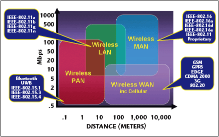
Advanced 3G standards pose significant technical challenges to system designers and product architects from several aspects. The radio itself is much more advanced, requiring higher performance components. Applications, such as video, demand increasingly sophisticated circuitry, and the expected usage profile is very different from voice, placing additional demands on battery consumption. Making this even more difficult, new 3G phones need to be backward compatible with the older GSM and CDMA networks in order to ensure coverage and seamless handover. Additionally, they cannot be significantly larger than last generation phones and need to have similar talk and standby battery lifetime. Recent developments in wireless communications have also resulted in handheld cellular phones that can utilize up to seven different wireless standards or bands including DCS, PCS, GSM, EGSM, CDMA, WCDMA, GPS and Wi-Fi. Each standard has its own unique characteristics and constraints, and brings with it its own specific challenges. Radio frequency microelectromechanical systems (RF-MEMS) may help engineers design phones that meet the challenges of integrating multiple bands while maintaining long battery life and progressively reducing the overall size of the handset as well as adding new capabilities, while keeping these devices small and affordable.
Approximately 75 percent of the 100 or so components in a mobile phone are “passive” elements such as inductors, variable capacitors and filter devices. MEMS versions of these components promise to make phones more reliable and power efficient. If they succeed, say the industry analysts at Cahners In-Stat Group, the market for RF-MEMS is expected to grow to nearly $350 million in 2006. Analysts at MegaTech Resources predict the quantitative model forecasts to reach $100 billion in worldwide MEMS shipments in 2010. The long-term potential is estimated at $2 trillion by 2025.
Trends
From a design standpoint, the evolving definition of 3G handsets requires an increasing focus on power consumption, space and architectural efficiency. Perhaps the biggest change, at least from an RF standpoint, is the requirement for multiband and multimode operation (see Figure 1). Meeting the stringent RF standards for several bands and technologies has greatly increased the complexity of the RF front-end. For example, European phones are expected to support at least three bands (900, 1800 and 2100 MHz) and two dissimilar technologies (GSM and WCDMA), not withstanding the addition of WLAN, Bluetooth or GPS, etc., in higher end handsets. Each technology requires its own specific filters designed for specific bands, making the front-end complex, large and costly. Making matters worse, adding switches or other components at the front-end of the phone to efficiently route signals creates loss and distortion that may impair performance or increase power consumption. Anything inserted between the antenna and the first low noise amplifier (LNA) results in a higher noise figure, which impacts overall radio sensitivity. Moreover, the active battery life is heavily influenced by the power consumption of the power amplifier (PA). Simply put, any loss in front of the PA will dissipate power that should go out the antenna, further reducing battery life. Perhaps less obvious is the fact that successive generations of wireless standards have sought to eke out more efficiency from the limited spectrum by using more complex signal waveforms. While this certainly places demands on baseband processing, the advancing sophistication of digital circuits has kept pace, if not driven, the evolution of wireless modulation and coding technologies. However, these increasingly complex signals require very linear RF components in order to limit distortion and ensure high signal throughput. A practical example of this is the extensive use of GaAs power amplifiers in most CDMA handsets. Despite efforts to integrate PAs into the transceiver, these components have remained external, largely due to the constraints of maintaining linearity at high power levels across wide frequency bands. What is needed is a technology that can deliver low loss with excellent linearity, while drawing no additional power and occupying the smallest possible area. Ideally it should be capable of further integration with a transceiver or other active components. Figure 2 shows the complexity of an RF front-end as additional frequency bands and RF technologies are included. This growing complexity enables tunable RF solutions with RF-MEMS switch and filter technologies that simplify this architecture.

MEMS technology is a leading candidate to address this emergent problem. RF-MEMS uses microscopic moving structures that are built using silicon chip manufacturing technologies. MEMS devices are not new and have found widespread application in airbag sensors, accelerometers, micro-optics, video projection systems and printer heads, to name but a few.
Using the integration of mechanical elements, actuators and circuits on a common silicon substrate, MEMS devices are built through micro-fabrication technology. While electronics are fabricated using integrated circuit (IC) process sequences (such as CMOS, bipolar or BICMOS processes), MEMS components are fabricated using “micro-machining” processes that selectively etch away parts of the silicon wafer or add new structural layers to form tiny mechanical and electromechanical devices. RF-MEMS-based devices are tiny, almost perfect physical switches, with none of the inherent limitations of semiconductor-based switch technology. Therefore, they reduce space and cost while simultaneously achieving a combination of high isolation and low insertion loss that is unachievable with conventional silicon technology. MEMS-based RF components can thus improve performance, while reducing power consumption and lowering cost, all critical factors in the front-end components of cellular phones as well as other high performance RF applications. It is worth noting that there are already MEMS-based components in cellular phones. Both surface acoustic wave (SAW) filters and film bulk acoustic resonance (FBAR) filter devices are forms of MEMS devices. FBAR, in particular, is a worthy example of a technology that is simple to create, but took years of perfecting before it became practical in terms of performance, cost and yield for cellular phone applications. FBAR devices, now featured in most CDMA phones, exhibit good performance at a very low height profile. This reduced height made them an essential choice, driving the volumes of FBAR devices produced up and costs down. Several manufacturers now have FBAR and bulk acoustic wave (BAW) filters in production and they are finding significant favor in today’s smaller and thinner phones. Figure 3 shows a high resolution image of an actual RF-MEMS structure that can be used as a building block for filters similar to FBAR.

Problems to Overcome
RF-MEMS switches have been in development for several years, but like all new and potentially disruptive technologies, there are several key problems to overcome. Initial developments of RF-MEMS switches were focused on the very fast T/R switch that is used in all GSM phones. However, while significant advances have been made, the very mechanical nature of MEMS devices limits its switching speed. It may still be possible for MEMS devices to meet GSM specifications, but not easily or without compromising cost or performance in other areas. As with FBAR devices, however, the application has serendipitously evolved into the sweet spot for RF-MEMS, rather than the other way around. The need for multiband, multimode switching, with low insertion loss while maintaining excellent linearity for WCDMA or CDMA signals, is driving the need for RF-MEMS-based devices. The problem and the value of the solution are only expected to increase as new and more complex waveforms such as WiMAX are added to the mix. Being essentially broadband devices, RF-MEMS switches are far less affected by frequency than semiconductor solutions and are more suitable at even higher frequency bands. This makes a front-end based on this technology a very adaptable platform, saving design time, cost and speeding time to market.
RF-MEMS for Software-defined Radio Applications
There is also significant interest in RF-MEMS for software-defined radio applications or those such as in the US Joint Tactical Radio System (JTRS) intended for first responders and other government and military users, where a reconfigurable front-end is part of the value proposition. Key problems still remain, however, largely in driving down costs and size. First, most MEMS devices are electrostatically activated, using relatively high voltages (20 to 80 V) to operate, but at infinitesimal currents. In the long run, this is really a system architecture problem since there is no reason why such a voltage could not be made available in a phone if the benefits are apparent at the system level. In the meantime, vendors are building charge pumps into their offerings in order to adapt them to current generation designs. Longer-term solutions involve monolithic integration of the control and charge circuitry into the MEMS devices themselves by building MEMS on top of active circuitry, or relocating the circuitry to other front-end components where the functionality can be absorbed on an incremental basis. This is particularly attractive in the context of highly integrated front-end modules. Also, as with SAW filters and FBAR devices, MEMS switches require a fair degree of hermeticity for reliable performance. MEMS devices are very sensitive to moisture, atmospheric particulates and other contaminants, which may interact with the contact surfaces. This means packaging the switches in a low cost, low profile, sealed package. This is the key problem for the MEMS industry to solve if it is to successfully intersect the high volume cellular phone world. The good news is that the SAW industry is already pioneering solutions that can be adapted to the needs of MEMS devices. SAWs originally started in ceramic packages and have progressed through flip-chip to chip-scale packaging, with wafer-scale packaging on the horizon. While the technology and needs of MEMS devices are slightly different, there is every reason to expect RF-MEMS devices to leverage the significant body of experience and low cost technology that has been perfected. Figure 4 shows how advanced semiconductor processing technology can permit MEMS devices to be sealed at the wafer level during manufacture, to provide hermetic encapsulation of the critical MEMS devices. This process simplifies device singulation and allows the use of standard packaging techniques. Subsequent over-molding provides additional strength and resilience, also ensuring long-term hermeticity.

The other main impediment to-date has been unproven reliability or the need to demonstrate in excess of 1011 (100 billion) cycles. This requirement was dictated by the fast switching T/R specification and while still valid, can be significantly relaxed if only band switching is contemplated, again making MEMS a more immediate prospect. In addition, MEMS devices have made significant strides in this area with numbers in excess of four billion cycles and, in some cases, being well beyond published results. The last requirement is adapting MEMS to low cost fabrication techniques that will lead to an intrinsically low cost base and will permit further integration. Initially MEMS devices were built in specialty shops, using custom MEMS processes in order to cater to very special needs and deliver products that were targeted at very high end applications. Now, companies such as WiSpry and others are building MEMS devices in standard high volume fabrications, using processes and material sets that are compatible with high volume CMOS manufacturing techniques. This not only leverages the significant infrastructure that exists in the semiconductor world, but ensures a path to further integration with active devices.
The Future of MEMS
It is this potential for integration that really excites the semiconductor world. FBAR devices, SAW filters, PIN diodes and GaAs components used in today’s cellular phones are all very much discrete technologies that, to-date, have resolutely resisted integration. Most of the innovation in size and cost reduction has taken place at the packaging level with the evolution of front-end modules (FEM) emerging as the key solution for many applications. MEMS devices offer a path to the integration of filter and switching technologies, creating a road map for intrinsic size and cost reduction for FEM providers and system architects.
As with previous technologies, volume dictates its own solutions and as the opportunity becomes apparent and measurable, companies are applying the resources to solve these last remaining hurdles to widespread adoption. A virtual circle of innovation and reward exists to be tapped.
These initial applications for RF-MEMS devices will undoubtedly lead to more advanced applications as this disruptive technology becomes more widely adopted and its benefits proven. Simple applications such as band select switches will lead to more complex and integrated solutions as MEMS technology is integrated into the silicon fabric itself.
System architectures will undoubtedly evolve where designers can take full advantages of the low loss, high linearity and essentially broadband operation capabilities that MEMS devices offer, designing around the capability to maximize performance or lower cost elsewhere in the design. The loss saved by using a MEMS switch may be just enough to enable a more efficient solution to be used elsewhere in the design, allowing the use of a CMOS LNA or PA instead of a SiGe or GaAs one. Doing so may allow even further integration of transceiver technology in association with a highly integrated MEMS-based front-end.
Looking forward, MEMS-based switches, switched filters and tunable filters will form key components in more integrated solutions. Tunable filter solutions based on MEMS devices simplify the design of front-end modules that need to support an increasing number of frequency bands and communication standards. They may also be used to create tunable structures integrated with other active components to create wideband power amplifiers, broadband tunable matching networks or adaptive antenna matching, giving rise to a new class of adaptive RF components. Similarly, MEMS devices may be used to vary the load impedance match of a power amplifier, ensuring it is operating at the highest possible efficiency at all power levels, thus improving power-added efficiency (PAE) and increasing battery life. The latter is an area of great interest to system designers, given that WCDMA phones are far less power efficient than the GSM ones they hope to replace. MEMS-based resonators are also being investigated heavily as a means to drive further integration of tunable or at least integratable filters into silicon devices. As the benefits of MEMS-based RF technology become evident and as the technology itself matures to the point where it can be integrated with other devices, new architectures are becoming possible that will take full advantage of the many capabilities that MEMS has to offer; as MEMS transform architectures through wide adoption, the industry is seeing great potential for RF designs in cellular and personal communications systems (PCS), wireless networking, the wireless Internet and other platforms that operate up to the mid-2 GHz range.
Mark Chapman is vice president of business development for WiSpry Inc. His past experience includes serving as the president and CEO of Ditrans Corp., and executive level positions for Comarco Wireless Technologies and Rockwell Semiconductor (now Conexant).