

Antennas are usually designed and simulated with powerful 3-D electromagnetic field solvers which designers use to investigate antenna performance such as input matching, gain, directivity, efficiency… Obviously, the performance will depend on the antenna itself but will also be a function of the feed network. Traditionally these two parts are simulated separately: the antenna’s feed network will be designed and optimized in a circuit simulation tool whereas the antenna will be designed in the 3-D electromagnetic field solver using a set of idealized inputs. Prototypes of both parts will be fabricated and tested separately to verify the specification of each part. Ultimately the two parts will be assembled for final testing. Whilst this methodology may work fine for simple devices, it may fail for complex antenna systems where the interaction between the antenna and its feed network cannot be neglected. In the latter case, modifications made once the physical hardware is created can be costly and time consuming. Fortunately modern software tools offer the opportunity to simulate both antenna and feed network simultaneously thanks to two-way Dynamic Link between circuit simulation and 3-D field solver tools. In this article, the two-way link between Ansoft Designer® circuit simulation and HFSS™ 3-D field solver tool, part of the Ansoft suite of products, from ANSYS Inc. will be described, and an electronically-scanned phased array example will be used to demonstrate how to evaluate the effect of power amplifier non linearity and thermal dissipation on the antenna radiation pattern, all within a single simulation framework.
Two-way link between circuit simulator and 3-D field solver.
A simple four by one patch array antenna, shown in Figure 1, will be used to describe the two-way link.

Figure 1: 9 ports 4x1 Patch array antenna
In the HFSS 3-D field solver simulator, far field radiation is computed from field values on the radiation boundaries using an infinite sphere, defined by two angles Phi and Theta, with respect to the signal levels specified at each source. Figure 2 shows the TotalGain at Phi=0 deg as a function of theta when a signal of magnitude 1 volt and phase 0 deg is set at each port whilst Figure 3 shows the case when the signal at ports 3 and 9 are set with a magnitude of 4 volts and a phase of 90 deg .

Figure 2: Radiation pattern and source signal level. All sources using 1V and 0 Deg.

Figure 3: Radiation pattern and source signal level. Source 3 and 9 using 4V and 90 Deg.
Ansoft Designer circuit simulator provides a powerful feature known as a “Dynamic Link” enabling direct use of the HFSS 3-D field solver project as a component in the circuit simulator. Figure 4 shows a circuit schematic where the 3-D field solver antenna array project is imported and used as a component. Ideal amplifiers and phase shifters are connected to the paths feeding each of the individual patch antennas and an AC source is used to drive the input of the circuit (Port:1).

Figure 4: 3-D field solver project imported in circuit simulator.
S parameter data from the 3-D field solver antenna array project is used during the simulation. The signals at the connection nodes between circuit and 3-D field solver project components are automatically probed and passed to the 3-D field solver project to setup source values and update near or far field quantities. This capability works with multiple types of analyses: Linear, Harmonic Balance and Transient analysis. Finally, near or far field quantities are passed back to the circuit simulator enabling plotting and optimization of field quantities from within the circuit simulation.
Using the circuit shown in Figure 4, optimization is setup to shape the gain of the patch antenna array. The following specifications are entered for antenna gain at 5.7 GHz:
• At Theta= 0 Deg: antenna gain ≥ 11 dB
• At Theta= 12 Deg: antenna gain ≤ 8 dB (Gain at -3 dB)
• At Theta= 41 Deg: -20 dB ≤ antenna gain ≤ -16 dB (side lobe gain)
For this optimization, only the ideal amplifier gain value will be used as an optimizable variable. Amplifier gain values are initially set as G1=0, G2=0, G3=G2 and G4=G1, and G1 and G2 can vary between 0 and 10dB. Optimization is performed using the Sequential Non Linear Programming algorithm with 10 iterations.

Figure 5: Antenna gain before (red) and after optimization (blue)
After 10 trials, the optimizer reached an improved solution: the realized gain increased by 2.58 dB, the -3dB gain is reached for Theta=13deg and side lobe rejection is -26.4 dB, see Figure 5. This example used ideal circuit models and linear circuit analysis and is intended to describe the process of establishing the two-way link between Ansoft Designer circuit simulator and HFSS 3-D field solver. The ability to do the same kind of analysis using harmonic balance simulation extends the scope of the analysis, using non-linear transistor models where the effect of gain and phase compression as well as temperature dependency of the transistor and the impact on the far field radiation can be evaluated. In the next part of this article, an electronically-scanned phased array antenna will be used to illustrate this process.
Phased Array Antenna System Design
The case study used in second part of this article is a phased array antenna system like those used on Unmanned Aerial Vehicles (UAV). The goal is to combine the simulation of the antenna and its electronic feed network. The phased array antenna is a group of antenna elements in which the relative amplitude and phase of the signal source on each element is varied dynamically to achieve a particular radiation pattern, enabling electronic beam scanning. Phase and amplitude weights are computed for a 16x16 element antenna array, see Figure 6(a). Figure 6(b) shows magnitudes for each of the 256 elements in the array when using a separable distribution, and applying a Taylor weighting to the element amplitudes, to ensure the first four sides lobes are suppressed to <-30 dB.

Figure 6: 16x16 element antenna array (a) and weighted magnitude for the 256 elements (b)
The center elements can be 15 dB higher in output power than the edge elements. The large dynamic range will have a strong impact on amplifier non linearity and thermal distribution. This case study will focus on the center row elements. A 1x16 element antenna array, see Figure 7, will be used with associated phase and amplitude weightings from one of the center rows.

Figure 7: 1x16 elements antenna array

Figure 8 shows the block diagram of the system for the 1x16 antenna array. The input signal is distributed through a power divider to each path feeding a single antenna element. Each path includes an attenuator, a phase shifter, a power amplifier and a circulator.
Figure 8: System block diagram
The attenuator and phase shifter form the beam forming network which sets the desired amplitude and phase for each antenna element. The power amplifier delivers the power needed to achieve the long range specification of the system. The circulator separates transmit and receive path. As only the transmit path is studied, the receive path is represented by a 50 ohm load. The system is built within Ansoft Designer circuit simulator using ideal element for the divider, attenuator, phase shifter and amplifier combined with the 1x16 antenna array HFSS project utilizing the “Dynamic Link”. Simulation with ideal components enables us to verify the computed values for phase and amplitude weights as well as verifying system sensitivity to parameter variations. The simulation shows a side lobe level (SLL) of around -29 dB, see Figure 9, verifying the specifications used for amplitude weight computation.

Figure 9: Antenna gain with ideal components
Ideal components will now be replaced, step by step, with real available components and the impact on the array pattern will be investigated.
Phase shifter and attenuator
The ideal phase shifter and attenuator are replaced by a 5-bit MMIC digital phase shifter and 5-bit MMIC digital attenuator respectively, designed using the UMS HB20P process. The digital phase shifter has a resolution of 11.25° and the digital attenuator a resolution of 0.5 dB. On Figure 10, the Δ parameter shows the difference between the computed value for the phase or amplitude and the achieved value with designed MMIC component.

Figure 10: Attenuator weight and phase value.
The attenuator model included a 0.5 dB bit which utilizes small resistor values from the UMS design kit. These small resistors create a poor match for the output of the attenuator when connected to the rest of the system. To reduce attenuator mismatch the last bit was removed and attenuator setting adjusted. The quantization and mismatch impact on the side lobe level (SLL) is about 5 dB higher than the ideal results, see Figure 11 (blue curve ideal, red curve with digital attenuator/phase shifter).

Figure 11: Antenna Gain- ideal element versus digital attenuator/phase shifter – SLL around 5 dB higher Power Amplifier
The power amplifier is an X band driver amplifier from UMS with a small signal Gain of 23 dB, an output power at 3 dB compression of 29.5 dBm and power added efficiency of 40%. The design of the power amplifier utilized the non-linear electro-thermal transistor model, from the UMS design kit. Thus the transistor model is temperature dependant enabling evaluation of thermal effects. In the real system, the amplifier die is mounted in a package, so the amplifier model will also include a 3-D model of a package simulated in HFSS, see Figure 12. The package model is combined with the transistor level model of the amplifier within Ansoft Designer circuit simulator and then inserted in the full system model.
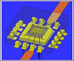
Figure 12: Amplifier package
The impact of the power amplifier and its package on SLL is about a 0.8 dB degradation. The final ideal component to be replaced is the 16-way power divider. The impact of amplifier non linearity will subsequently be evaluated.
16-way Divider
The 16-way divider, Figure 13, will be simulated in HFSS and included in Ansoft Designer thanks to the “dynamic Link”. The geometry of the 16-way divider needs to be optimized to minimize losses and mismatch. Optimizing the entire structure in the 3-D field solver is time consuming and not efficient, even when utilizing high performance computing (HPC) facilities available within HFSS and simple circuit optimization is not effective due to the non standard geometry of “T” junction. The best approach is to optimize a circuit consisting of parametric 3D field solver components.

Figure 13: HFSS project of the 16-way divider.
Figure 14 shows one stage of the 16-way divider implemented in the circuit simulator. Each component in the schematic, tee (a), bend (b) and transmission line (c), is connected to a pre-solved parametric HFSS project. Using these “dynamic links”, interpolation can be performed over the pre-solved design space in the 3-D field solver, which enables the speed of circuit simulation with the accuracy of physics based circuit models.
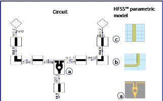
Figure 14: Parametric HFSS model in circuit simulator of a single divider stage.
For optimization in the circuit simulator, each stage of the divider has a reactive T element which has a variable hole radius and center location as well as variable feed line lengths resulting in a total of 8 unique design variables for the full design. Optimization is performed on the complete divider circuit providing specific values of hole radius, center location and feed line length for each stage of the divider. The parametric HFSS simulation of the tee junction is performed using the “distributed solve” technique in approximately 30 minutes and the final circuit simulator optimization takes around 10 minutes. As a final validation, the full divider model is then simulated in HFSS based on the optimized dimensions and compared to circuit simulator results showing very good agreement, see Figure 15.

Figure 15: Full divider in HFSS vs. Circuit simulator results
Insertion of the optimized 16-way divider in the full system simulation results in a further SLL degradation of around 1.8 dB. Comparison between circuit simulation using ideal components and virtual prototype simulation using all real components is shown in Figure 16, blue curve ideal, red curve virtual prototype.
Figure 16: (a) amplifier in linear region (b) amplifier in compression
Figure 16 (a) shows SLL is around 7.8 dB higher with amplifiers working in the linear region. At this step, where all the components are combined together, the impact of amplifier non linearity is evaluated by driving the power amplifiers into compression, the result shows SLL around 14 dB higher than the ideal model, see Figure 16 (b).
Full panel simulation
The impact of each component on the radiation performance of the antenna array has been evaluated with significant impact on the overall system performance observed when including real non-ideal component models. Due to the partitioning of the system simulation, potential coupling between parts cannot be identified in this manner. In addition, thermal effects can also be evaluated utilizing the link between HFSS and ANSYS® Mechanical™ and fed back to circuit simulation.

Figure 17: Final virtual prototype array panel in HFSS
The entire passive panel including radiating elements, circulators, packages, bondwires, and 16-way divider is run in HFSS, see Figure 17. The solved project of the entire passive panel is linked to the circuit models of the phase shifter, attenuator, and power amplifier, see Figure 17.
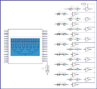
Figure 18: Ansoft Designer schematic with full panel and electronic circuit.
The link between HFSS and ANSYS Mechanical is used to compute the temperature distribution over the full panel and then feedback die temperatures to the non-linear circuit simulation by setting the temperature parameter of the non-linear electro-thermal transistor model. The full panel model from HFSS is exported to ANSYS Mechanical including geometry, material definition and losses computed from 3-D field solver simulation. The losses from 3-D field solver simulation are mapped to the mechanical mesh and boundaries and heat sources are setup within ANSYS Mechanical. The heat sources are defined at the location of each of the power amplifiers. The magnitude of each heat source was evaluated from output power, power added efficiency and bias levels quantities of the amplifiers taking into account the 15 dB dynamic range due to the amplitude weightings. Figure 19 shows simulation results within ANSYS Mechanical. The temperature distribution shows a difference of around 45 °C between the amplifiers in the center and at the edge of the panel.
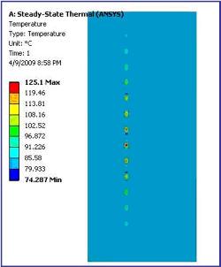
Figure 19: Thermal distribution of the full panel
The temperature values are manually identified from the thermal distribution and used to set the transistor temperature parameter in the circuit simulation shown in Figure 18. Figure 20 (a) shows the comparison between simulation where temperature parameter for all transistors is set to 25 °C and where temperature parameters is set using the thermal distribution, Fig 20 (b).

(a) (b) Figure 20: Full system simulation pattern (a) without temperature distribution (b) with temperature distribution
Simulations show that in this case, the temperature distribution does not significantly impact the full system simulation radiation pattern.
Conclusion
The two-way link between Ansoft Designer and HFSS demonstrated in the first part of the article enabled a new methodology for design of complex antenna systems. This new methodology can be described in four main steps. First the combination of ideal components used to model the feed network and the 3-D field solver simulation of the antenna array enables validation of the phase and amplitude weightings applied to each element of the antenna array. Second, by replacing ideal components with real designed components, effects such as quantization noise, mismatch, and amplifier non linearity can be identified and rectified to avoid full system performance degradation. Third, the ability to create and use 3-D field solver parametric model libraries within the circuit simulator enables evaluation of design trade-offs and identification of an optimal design with reduced simulation time and with accuracy of physics based circuit models. Finally, with the added benefit of the ANSYS Mechanical link to HFSS and Ansoft Designer, we can gain more insight into complex system designs before building prototypes by evaluating thermal effects on the overall system radiation pattern.
Thanks to Jim Delap, Nick Hirth, Markus Kopp, Dane Thompson and Andrew Wang of Ansoft. This advice column could not have been written without their contribution.
References
1) Williams L., Rousselle S. "Microwave Simulation Macro benefits" Ansys Advantage, Volume II, Issue 4, 2008
(2) Delap J. "RF Power Amplifier Design Using Coupled Circuit, EM, and Thermal" Smart Engineering Simulation™ – Application Workshops for Electronic Design, www.ansoft.com/electronicdesignworkshops