
In recent years, the 7 GHz of contiguous bandwidth have been opened for unlicensed use at millimeter-wave frequencies around 60 GHz (known as V-Band) in the US and Japan. High rate wireless communication technology operating at millimeter-wave frequencies has been an interesting topic with various applications and tremendous potentials. This led to a strong demand for RF circuits operating above 20 GHz. In the past, these frequency bands were dominated by III-V semiconductor technology, such as GaAs-based HEMT and HBT. However, the advantage of combining baseband and RF front-end on one single chip for cost savings is strongly desired for highly integrated system-on-chip (SOC) applications. Thus, the CMOS process is one of the most attractive solutions to implement RFICs because of its low cost and high level of integration. Recent works have proven that the CMOS process is a promising technology for RF circuits in low GHz applications. Due to the advancement of the CMOS process, the improvement of the unity gain frequency fT of CMOS devices suggests a potential for utilizing the CMOS process in millimeter-wave applications.
Recently, efforts to design millimeter-wave amplifiers by using CMOS processes have been reported, using 0.13 μm and 90 nm CMOS.1-3 In this article, the aim of this work is to design a V-Band, low noise amplifier that is suitable for SoC and wireless communication systems. It achieves a peak gain of 11.7 dB while consuming 21.6 mW.
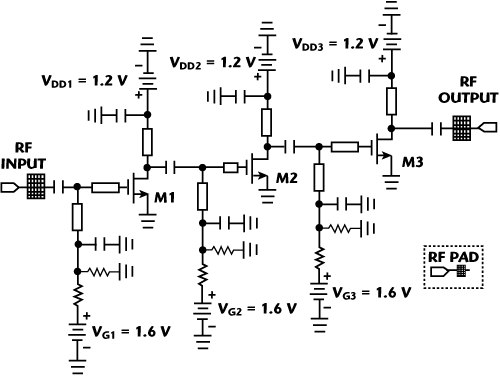
Figure 1 Schematic V-Band CMOS LNA.
V-band LNA Circuit Design
This circuit was fabricated in commercial standard 0.13 μm 1P8M CMOS process. Passive elements, including metal-insulator-metal (MIM) capacitors, are available between metal 7 and 8. The schematic of the three-stage cascaded common source V-Band LNA is shown in Figure 1. Generally, the noise factor (F) of a common source amplifier is usually defined as:

Figure 2 Comparison of MSG and NF of different cascade and CS transistors.
From Equation 1, the noise factor is proportional to ω0 and inversely proportional to Qin as well as ωT. The fT of a CMOS 0.13 μm NMOS transistor is approximately 91 GHz.2 Figure 2 illustrates the tradeoffs between the common source (CS) and cascode structures. In order to obtain a lower noise figure, a common source structure is adopted. In addition, the sizes of the transistors are chosen under the consideration of low power consumption, while maintaining a desired circuit performance. The optimal width for the low noise input stage is 18 fingers with a total gate width of 36 μm, corresponding to a current density of 167 μA/μm with a supply voltage of 1.2 V and gate bias of 0.8 V.
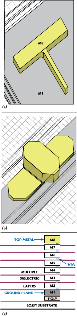
Figure 3 (a) Modeled T-junction, (b) cross-junction and (c) 0.13 μm cross-section.
In this work, a thin-film microstrip (TFMS) line is used for the matching networks and all interconnections. The TFMS consists of the top metal layer (M8) as the signal microstrip lines and the first metal layer (M1) as the ground plane. As compared to coplanar waveguide (CPW), microstrip lines have more flexibility in interconnection. All of the T-junctions and cross junctions were realized using the same structure, as shown in Figure 3, modeled with a FEM-based 3D full-wave EM solver, Ansoft HFSS.
As CMOS technologies advanced beyond the 0.18 μm node, increasingly stringent metal density rules prohibited the design of solid ground planes. In order to accommodate these restrictions, metal ground planes must now be slotted.5 Figure 4 shows the simulated effective permittivity of the TFMS. It illustrates good agreements between our simulation and Mangan's work5 under the same conditions. Thus, the reasonable effective permittivity applied to this work is chosen as 3.6.
Measurement Technique and Results
The chip micrograph of the fabricated CMOS LNA is shown in Figure 5 and the chip size is 1.39 × 0.76 mm. The LNA was measured on-wafer, using high frequency probes. The VDD supply voltage and gate bias voltage were 1.2 and 0.8 V, respectively. The parasitic effects of the RF pads were incorporated while performing simulation, so no de-embedding was required on the measured results. The measurement of millimeter-wave components needs a complex calibration procedure. For example, the available input power from the source is calibrated with a V-Band power sensor (Agilent V8486A) and the frequency dependent loss from the probe loss should be calibrated also. Measurement of noise figure at V-Band or higher frequencies is a challenge. In the measurement, the cable losses, probe losses and DUT intrinsic noise are all measured by a noise figure analyzer (NFA) under testing.
Using the Friis' formula, Fmeas can be defined as:

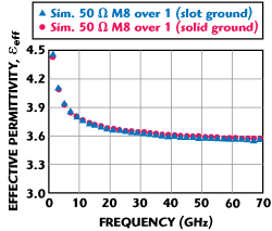
Figure 4 Simulated effective permittivity of TFMS line with a metal 8 conductor in the 0.13 μm process.
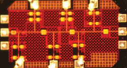
Figure 5 Photograph of the V-Band three-stage CMOS LNA.
where, F1 is the noise figure of the input cable and input G-S-G probe (which is equivalent to the loss of the cable and the probe, L1=G1-1). Similarly, F3 is the noise figure of the output cable and output G-S-G probe. From Equation 2, if the GLNA is high enough, the FLNA can be approximated as:
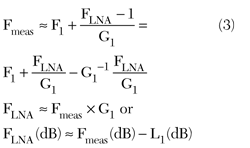
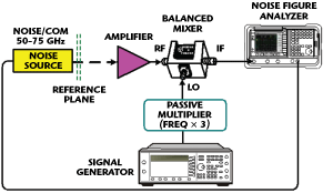
Figure 6 Calibration of the NFA with the V-Band noise source, amplifier and down-converter.
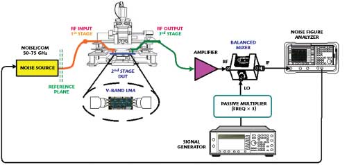
Figure 7 V-Band noise figure measurement system.
From Equation 3, if the loss of the first stage is known, the additional noise can be calibrated out. Figure 6 shows the calibration of the NFA together with the V-Band noise source, amplifier and down-converter. The V-Band noise figure measurement system is shown in Figure 7 and a photograph of the on-wafer measurement set-up is shown in Figure 8.
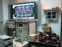
Figure 8 Photograph of the on-wafer measurement system.

Figure 9 Measured input (S21) and output (S22) return losses.
The LNA was measured on-wafer using high frequency probes. The VDD supply voltage and gate bias voltage were 1.2 and 0.8 V, respectively. The parasitic effects of the RF pads were incorporated while performing simulation, so no de-embedding was required on the measured results. The measured input and output return loss are plotted in Figure 9. The input and output return losses were close to 9.4 and 16 dB, respectively. Figure 10 shows that the small signal gain is 11.7 dB at 50 GHz with a noise figure of 7.9 dB, while consuming 21.6 mW from a 1.2 V supply. The 3 dB bandwidth is 6 GHz. As shown in Figure 11, the measured input 1 dB compression point (P1dB) is -9.5 dBm.
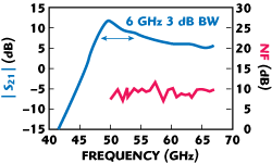
Figure 10 Measured gain and noise figure.

Figure 11 Measured input 1 dB compression point.
Conclusion
This article presented the design, fabrication and measurement of a proposed V-Band LNA. It was fabricated in a TSMC 0.13 μm standard CMOS process. Compared to other works using 0.13 μm CMOS, this work has shown that the V-Band LNA reduced the power consumption successfully. The circuit was measured using on-wafer probing. The V-Band LNA has demonstrated a gain of 11.7 dB, a minimum noise figure of 7.9 dB. The input P1dB is -9.5 dBm and IIP3 is -1.65 dBm. The total power consumption is 21.6 mW from a 1.2 V power supply.
Acknowledgment
This work is supported by the National Science Council, Taiwan. The authors would like to thank the Chip Implementation Center (CIC) of National Science Council, Taiwan, China, for supporting the TSMC CMOS process.
References
- C.H. Doan, S. Emami, A.M. Niknejad and R.W. Broderson, "Millimeter-wave CMOS design," IEEE Journal of Solid-State Circuit, Vol. 40, No. 1, January 2005, pp. 144-155.
- C.M. Lo, C.S. Lin and H. Wang, "A Miniature V-band 3-stage Cascode LNA in 0.13 m CMOS," 2006 ISSCC Digest of Technical Papers, pp. 1254-1263.
- T. Yao, M. Gordon, K. Yau, M.T. Yang and S.P. Voinigescu, "60-GHz PA and LNA in 90 nm RF CMOS," 2006 IEEE RFIC Symposium Digest.
- H.O. Vickes, M. Ferndahl, A. Masud and H. Zirath, "The Influence of the Gate Leakage Current and the Gate Resistance on the Noise and Gain Performances of 90-nm CMOS for Micro- and Millimeter-wave Frequencies," 2004 IEEE MTT-S International Microwave Symposium Digest, Vol. 2, pp. 971-974.
- A.M. Mangan, S.P. Voinigescu, M.T. Yang and M. Tazlauanu, "De-embedding Transmission Line Measurements for Accurate Modeling of IC design," IEEE Transactions on Electron Devices, Vol. 53, No. 2, February 2006, pp. 235-241.
- C.L. Ko, C.N. Kuo and Y.Z. Juang, "On-chip Transmission Line Modeling and Applications to Millimeter-wave Circuit Design in 0.13 μm CMOS Technology," 2007 IEEE International Symposium on VLSI Design, Automation and Test Digest, pp. 1-4.
- C. Inui, I.C.H. Lai and M. Fujishima, "60 GHz CMOS Current-reuse Cascade Amplifier," Proceedings of the 2007 IEEE Asia Pacific Microwave Conference, pp. 793-796.
- S. Pellerano, Y. Palaskas and K. Soumyanath, "A 64 GHz 6.5 dB NF 15.5 dB Gain LNA in 90 nm CMOS," Proceedings of the 1998 IEEE AP-S International Symposium, Vol. 2, pp. 676-679.
Hsin-Chih Kuo received his bachelor's degree in electrical engineering from Feng Chia University, Taichung, Taiwan, in 2006, and his master's degree from the Institute of Computer and Communication Engineering, Department of Electrical Engineering, National Cheng Kung University, Tainan, Taiwan, in 2008. His research interests include millimeter-wave RFIC and RF system design.
Chu-Yun Yang received her bachelor's degree in electrical engineering from Yuan Ze University, Taoyuan, Taiwan, China, in 2008. She is pursuing a master's degree in the Institute of Computer and Communication Engineering, Department of Electrical Engineering, National Cheng Kung University, Tainan, Taiwan. Her research interests include the microwave and millimeter-wave RFIC design.
Huey-Ru Chuang received his bachelor's and master's degrees in electrical engineering from the National Taiwan University, Taipei, Taiwan, China, in 1977 and 1980, respectively, and his doctorate in electrical engineering from Michigan State University, East Lansing, MI, in 1987. He is a professor in the Institute of Computer and Communication Engineering, Department of Electrical Engineering, National Cheng Kung University, Tainan, Taiwan. His research interests include wireless RF/microwave circuits and millimeter-wave RFIC design, microwave communication and detection systems, and wireless communication antenna design.