
The rapid growth of wireless communications, as well as space-borne systems, leads to the increasing demand of low power, high efficiency systems. High efficiency is the prime requirement for any space-qualified transmitter or wireless communication systems. Higher efficiency means greater output power with reduced power dissipation. Achieving higher efficiency necessitates the active device to run into heavy saturation, leading to highly nonlinear behavior. In contrast to linear classes of amplifier (Class A, B, AB), which have efficiencies of the order of 40 percent, nonlinear switched mode amplifiers (Class D, E, F) offer efficiency better than 60 percent. Among the switched mode schemes, Class E power amplifier requires a fast switching signal, which is not required in Class F operation. Class F is preferred over Class E due to large switching stress on the active device in Class E operation. This power amplifier will be used as the final power stage of the solid-state power amplifier (SSPA) for the Chandrayaan-II mission.

Figure 1 Schematic of a Class F amplifier.

Figure 2 Drain voltage and current waveform of an ideal Class F amplifier.
General Theory of Class F Amplifier
A Class F amplifier is a reduced angle amplifier with load harmonic tuning to shape the drain voltage and current in a way that they do not coincide or rarely coincide with each other, thus greatly reducing the power dissipated by the device. Theoretically 100 percent drain efficiency can be achieved using an infinite number of harmonic traps. The load must be a short at even harmonics and open at odd harmonics.1 Thus the drain voltage approximates a square waveform and the drain current, a half wave sinusoid. The two waveforms get displaced in the time domain so as to ensure zero drain current with drain voltage peaking and vice versa. As shown in Figure 1, the output network consists of a quarter wavelength transmission line and a parallel LC tank circuit tuned to resonate at f0. At f0, a pure resistive load R is seen by the drain as the tank circuit offers infinite impedance at f0. At even harmonics, the tank becomes a short and the quarter wave transformer appears to be of length of nλg/2, (g being the guided wavelength of the transmission line), thereby providing a short at all even harmonics. This results in a half wave rectified sinusoid drain current. For odd harmonics, the output tank becomes a short again and transmission line appears to be of length (2n + 1) λg/4, thereby transforming the short to an open circuit to the drain. The drain voltage contains only the odd harmonics and results in a square waveform as represented in Figure 2. All the harmonics contain either voltage or current and not both, therefore no harmonic power is generated by the active device. This confirms the realization of 100 percent efficiency, with the assumption that the active device is an ideal switch with no loss and zero output drain capacitance.
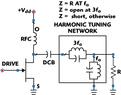
Figure 3 Third harmonic peaking.
Practical Design Constraints
In practice, only a limited number of harmonic terminations can be implemented. The active device has a finite bandwidth, which limits switching speed. This also limits the number of harmonics present. Thus, the design of the output network is implemented considering a tradeoff between efficiency and size. The maximally flat description2 shows that the lower order frequency components in the Fourier representation of a signal have the most effect on shaping the signal. Thus for practical design, only the second and third order harmonics are considered. In that case, the output network replaces the quarter wave transformer by another parallel tank circuit tuned at 3f0 as shown in Figure 3. Realizing this circuit with lumped components would introduce losses inherent to the high frequency lumped components. Instead, by taking advantage of impedance transformation properties of quarter wave long microstrip stubs, an equivalent circuit can be realized using a planar microstrip network.

Figure 4 Schematic of a Class F power amplifier.

Figure 5 Load harmonic trapping circuit.
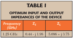
Design of Class F Amplifier
An RFMD GaN HEMT device RF3932 has been used to design this amplifier. Using the nonlinear model of the device, the optimum input and output impedance of the device has been found using the ADS load-pull utility. The optimum input and output impedance of the device as found from load-pull simulation are shown in Table 1. Figure 4 shows the schematic circuit of the overall amplifier. The input matching circuit of this amplifier is conventional and serves the general purpose of extracting maximum gain out of the device. The output matching circuit of the power amplifier consists of two parts: the harmonic trapping circuit and the fundamental matching circuit. The harmonic trapping circuit, as shown in Figure 5, consists of a short circuited stub (TL2) of length 90° at 1.25 GHz connected to the drain port. This stub presents a short circuit at the second harmonic and also provides the DC drain bias voltage. Thus the second harmonic is added to the drain current, thereby flattening the drain current waveform to approximate a half sinusoid signal. The series lines TL1 and TL3 along with Tee1 constitute a track length of 30° at 1.25 GHz. This, combined with an open circuited stub (TL4) of length 30° at 1.25 GHz, provides an open circuit at the third harmonic. Thus the third harmonic is peaked and added to the drain voltage, giving it the shape of an approximated square wave. The harmonic trap circuit is then followed by a fundamental matching circuit to ensure optimum power match between the drain impedance and the resistive load at f0. Figure 6 shows the drain impedance provided by the harmonic trapping circuit. The theoretical design is carried out for a single frequency, so an initial performance optimization was carried out to achieve a satisfactory simulated performance over the band of interest. Subsequently, a yield analysis was carried out to assess the initial yield and thereafter the yield was optimized to more than 85 percent to ensure that the design sensitivity is within ±20 micron with respect to the nominal value. Momentum simulation for EM analysis has also been carried out to consider parasitic coupling effects in the circuit.

Figure 6 Drain impedance over frequency.
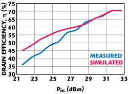
Figure 7 Drain efficiency (%) of the amplifier.
Design Validation
The amplifier, designed as per Class F approach, has been fabricated using an alumina 25 mil thick substrate εr = 9.9) and was tested for a pulsed RF condition, with a pulse width of 80 μs and a duty cycle of 24 percent. However, the amplifier can also be operated in CW condition with proper thermal design as the device is rated for continuous operation. The simulated and test results of the amplifier are shown in Figures 7 to 9. Also, a comparison of linearity performance between a Class AB and a Class F amplifier is presented in Figures 10 and 11.

Figure 8 Gain (dB) and Pout (dBm) of the amplifier.

Figure 9 Drain voltage and current waveform.

Figure 10 AM to PM conversion of Class AB amplifier.

Figure 11 AM to PM conversion of Class F amplifier.
Output Power and Efficiency
The test results of the implemented Class F amplifier show an output power of 47.8 dBm (60 W) at 70 percent drain efficiency. The active device RF3932 has the capability to produce 70 W power at hard saturation (4 dB compression), if biased at its nominal quiescent voltage and current rating (48 V, 220 mA). To ensure reliability over a long period of satellite operation, stress on the device is reduced by applying a drain bias of 45 V. Hence the saturated power of the device is reduced to 60 W, without compromising the efficiency. Figures 7 and 8 represent the drain efficiency, output power and gain of the amplifier, respectively, at 45 V drain bias as a function of swept input power.
Drain Voltage and Current Waveform
Figure 9 represents the voltage and current waveform of the GaN amplifier, probed at the drain lead of the packaged device. As expected in Class F operation, the amplifier has drain voltage and current waveforms such that their peaks occurred at different time, thereby reducing the power dissipation of the amplifier and increasing its efficiency. Table 2 represents the overall performance of the presented 60 W Class F power amplifier.


Figure 12 60 W Class AB amplifier.
Comparison of Linearity Performance
To compare the linearity performance between Class AB and Class F amplifiers, a Class AB amplifier is also designed and fabricated using the same active device RF3932, with a goal to achieve the same specification as in Table 1 (except the efficiency, which is bound to be lower in a Class AB operation). The linearity performance of the two amplifiers was measured in terms of the AM to PM conversion function (degree/dB) for both the amplifiers. Figures 10 and 11 represent the simulated and measured AM to PM conversion of the Class AB and Class F amplifiers. As expected, in Class F amplifier, higher efficiency is achieved, compromising the linearity of the amplifier. The Class F amplifier implemented exhibits a worst-case phase variation of +7.5°/dB to -4°/dB over the entire frequency band of 100 MHz, as compared to a phase variation of 1.2°/dB for the Class AB amplifier. The fabricated hardwares of the 60 W Class AB and Class F power amplifiers are shown in Figure 12, respectively. Table 38 shows a comparison of the performance reported in the literature for high efficiency amplifiers operating in the same frequency region with that of the present Class F amplifier.

Conclusion
A 60 W power amplifier, based on Class F architecture at 1.25 GHz ± 50 MHz, using a packaged GaN HEMT device, RF3932, is presented. The test results are showing very close match with the simulated results and validates the design of the 60 W power amplifier with 15 dB compressed gain and 70 percent drain efficiency. The design utilizes a planar microstrip line load network, with harmonic traps for second and third harmonics only. The nonlinearity of the Class F amplifier is higher than the Class AB amplifier, which is confirmed by comparing the AM to PM conversion test results.
Acknowledgment
The authors are grateful to the mechanical and PCB fabrication facilities. The authors are thankful to Shri Santanu Chowdhury, Group Director of AIPG, Dr. P.K. Srivastava, Deputy Director of SIPA, and Shri Tapan Misra, Deputy Director of MRSA, for their valuable suggestions. The authors are also very grateful to Dr. R.R. Navalgund, Director, SAC, for motivating and encouraging them to write this article and allowing us to present and publish it. The authors express their sincere thanks to RFMD India Inc. for their support.
References
- F.H. Raab, "Maximum Efficiency and Output of Class F Amplifiers," IEEE Transactions on Microwave Theory and Techniques, Vol. 49, No. 6, June 2001, pp. 1162-1166.
- F.H. Raab, "Class F Power Amplifiers with Maximally Flat Waveforms," IEEE Transactions on Microwave Theory and Techniques, Vol. 45, No. 11, November 1997, pp. 2007-2012.
- Tian He and Uma Balaji, "Design of a Class F Power Amplifier," PIERS Online, Vol. 6, No. 2, 2010.
- S. Gao, P. Butterworth, S. Ooi and A. Sambell, "High-efficiency Power Amplifier Design Including Input Harmonic Termination," IEEE Microwave Wireless and Components Letters, Vol. 16, No. 2, February 1997, pp. 81-83.
- D. Schemelzer and S. Lang, "A GaN HEMT Class F Amplifier at 2 GHz with 80% PAE," 2006 IEEE Compound Semiconductor IC Symposium Digest, pp. 96-99.
- Y.Y. Woo, Y. Yang and B. Kim, "Analysis and Experiments for High Efficiency Class F and Inverse Class F Power Amplifiers," IEEE Transactions on Microwave Theory and Techniques, Vol. 54, No. 5, May 2006, pp. 1969-1974.
- S.C. Cripps, "RF Power Amplifier for Wireless Communications," Artech House Inc., Norwood, MA, 1999.
- W.N. Edelstein, C. Andricos, F. Wang and B. Rutledge, "High-Efficiency L-band T/R Module: Development Results," Earth Sun System Technology Conference (ESTC), College Park, MD, June 28-30, 2005.
Suman Aich received his bachelor's degree in electronics and communication engineering from IIEST, Shibpur, WB, India, in 2008. Since September 2008, he has been working in SAC/ISRO as a Microwave Passive and Active Circuit Designer on pulsed SSPAs and transmitters for microwave remote sensing payloads. His research interests include the design of high efficiency transmitters and active and passive microwave components.