

Figure 1 Miniature quad hybrid coupler made with the Multi-Mix® process.
The following article describes a process for microwave, multi-layer integrated circuits and micro-multi-function modules (MMFM™) based on fluoropolymer composite substrates called Multi-Mix®. The fusion bonding of multi-layer structures provides a homogeneous dielectric medium for superior electrical performance at microwave frequencies. The bonded layers may incorporate embedded semiconductor devices, etched resistors, passive circuit elements and plated-through via holes, to form a 3D subsystem enclosure that requires no further packaging. In fact, the structure is the package. The small-footprint, low profile units are rugged, lightweight and with the various external interfaces, make it compatible with most RF structures (see Figure 1).
The process controls for the described method allow a low cost manufacturing approach that is suitable for high or low volume production. The platform strategy of MMFM modeling and simulation reduces engineering cycle time and enables the resulting product to be an economical solution for new circuit designs. Some of the benefits of the technology process include:
- High density circuit integration
- Industry-leading electrical and mechanical performance
- Improved quality
- Size and weight reduction
- Reduced cost
- High yield and full panel utilization
- Increased reliability over other techniques
- Adaptable for millimeter-wave applications.

Figure 2 Sub-miniature quad 3 dB hybrid coupler.
Figure 2 shows an example of a sub-miniature quad 3 dB hybrid with low loss of 0.35 dB, high isolation of 20 dB, power handling of 30 W operating from 800 to 1000 MHz. The device has good amplitude and phase tracking in a surface-mount structure that can be handled via tape and reel. Figure 3 shows the performance graphs for key parameters, including coupling, isolation, return loss and phase balance.
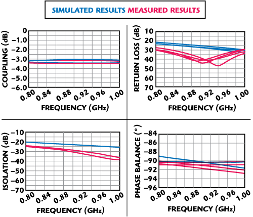
Figure 3 Simulated and measured results for quad 3 dB hybrid coupler.
The homogeneous medium of the process is also well-suited for the beamformers found in applications, such as phased array antennas, where the stability of the material allows for the addition of low Dk foams to form dipoles and patch antennas. In addition, process support for surface-mount components, such as circulators, resistors and other components, can be added to create a highly integrated structure.

Figure 4 Filter bank.
One example of the size and weight reduction made possible through this process is a S/C-Band multi-channel filter bank shown in Figure 4. In this filter, six multi-layer boards comprise the assembly. There are 14 contiguous filter channels distributed over three circuit substrates separated by three dielectric and ground plane spacers. After fusion bonding and edge plating, the finished assembly is approximately 3" × 4" × 3/8" and weighs less than 2 ounces. The multi-layer package replaced a considerably larger and heavier solution. The weight is now measured in ounces as opposed to pounds.

Figure 5 Quad hybrid multi-layer construction and performance data (a) compared to traditional design (b).
The Process in Detail
The process begins with commercially available polytetrafluoroethylene (PTFE) composite, copper-clad laminate material having inherently low dielectric loss and stable microwave properties. A low Z-axis coefficient of thermal expansion (CTE), close to that of copper and aluminum, ensures excellent reliability of plated-through holes and blind and buried vias. Controlled XY-plane thermal expansion, together with a low modulus, affords excellent reliability of surface-mounted devices in the most severe thermal cycling and thermal shock environments. Further, a low and uniform thermal coefficient of dielectric constant, coupled with the low CTE, result in consistent electrical performance over a wide operating temperature range and operating frequency. Figure 5 shows a traditional quad hybrid compared to one produced with the Multi-Mix process, which realized a 18× reduction in volume.
Complex microwave circuit patterns and transmission-line geometries may be chemically photoetched on the copper, maintaining dimensional tolerances of ±0.0005 inch. The incorporation of thin metal-film etched resistors is under qualification and will be available in the near future. Indexing holes for layer-to-layer alignment in assembly are precision machined or drilled into each board. Layer-to-layer plated-through holes (blind and buried vias) may be realized with a minimum diameter of 0.008 inch and aspect ratios of 6:1. Stacked layers can be fusion bonded directly to copper or aluminum plates offering exceptional thermal dissipation for the structure.
Active device attachments are embedded in cover layer cavities to provide environmental protection and allow pre-cap inspection and test. The pick and place of discrete components can be demonstrated on array panels up to 12 × 18 inches, with the potential to accommodate flip chip packages and ball grid arrays. Operating-frequency capability of current circuit designs range from VHF through Ka-Band. Properly sized and spaced blind and buried vias are used between ground planes to isolate lines and other RF structures within a ground plane. The ability to offer a high degree of isolation within a given layer allows a designer to run various signal traces on the same layer, reducing size without the worry of cross-talk or unwanted resonance. In fabricating a bonded multi-layer assembly, the stacked layers are placed in a fixture to which carefully controlled, uniform pressure and temperature is applied to meet the substrate fusion bonding requirements. After cooling and removal from the fixture, edge plating for EMI shielding and ground-plane integrity is performed. Finish plating layers for environmental protection include annealed matte tin, tin/lead and electrolytic nickel/gold.
Platform Strategy of Module Architecture
Whether it is for military or commercial applications, improved electronic design automation (EDA) modeling/simulation tools have been developed for microwave and millimeter-wave circuits and packages in order to support the RF/microwave circuit designer. Integrated mathematical, electromagnetic, thermal and mechanical modeling capabilities allow total package analysis to be performed prior to actual hardware fabrication, resulting in rapid turn-around and lower-cost prototypes.
It is important for RF designers to have access to simulation models that accurately represent the electrical behavior of the physical module. The module architecture described in this article utilizes a structural template, which overlays outlines and creates common interconnection paths. Process steps are based on design guidelines for each layer of a multi-layer microwave assembly. Actual test data for functional layer blocks are stored in a pre-designed library. Ansoft HFSS software has been utilized to provide the designer with access to S-parameter data for the purpose of predicting system performance, thus permitting co-design database availability. Experience with this approach thus far has been met with a high level of positive feedback. Complete design concepts from schematic to circuit layout and test may be performed within a single operating environment. Functional components may be inserted utilizing drag-and-drop techniques from ADS for insertion into system designs, which can be tailored for a specific application.

Figure 6 6 to 7.5 GHz multi-layer switch filter bank footprint (a) and performance data (b).
Multi-layer Integrated Circuit Considerations
To meet rigid system specifications, a multi-layer integrated circuit process for RF/microwave applications must maintain tight dimensional tolerances in the fabrication process to enable circuits with reproducible characteristics. Such a process should lend itself to an almost unlimited number of microwave component and subsystem product designs, including lowpass, highpass and bandpass filters, power dividers, couplers, delay lines and impedance transformers. These RF functional blocks will allow a designer to create more complex antenna feed distribution networks, array beamformers or comparators for monopulse receiving systems. Integration of beam-lead receiver or detector diodes in singles, pairs, quads or multi-ring configurations enable the manufacture of mixers and modulators to satisfy a broad range of application requirements in radar, electronic warfare and commercial communications systems. As an example, Figure 6a shows the footprint and Figure 6b the performance data of a multi-layer switch filter bank used in various applications.

Figure 7 Integrated power amplifier module.
Support for additional signal control and power conditioning devices, such as digital attenuators, limiters and switch matrices that may be prepackaged with their driver circuitry and embedded in cover layer cavities within the multi-layer assembly, allows designers to further reduce the physical footprint of the overall module. Interfacing each device with its necessary RF transmission lines and video/bias traces to external connectors is accomplished during the product design and layout phase. Connectorized assembly products typically utilize SMA, SMP, SSMP and SSSMP along with Corning Gilbert's line of connectors.
Active devices, including amplifiers, oscillators, frequency multipliers and dividers, can also be integrated in this manner. An example of this higher level integration is an amplifier module shown in Figure 7. High isolation is maintained between parallel conductors and between adjacent multi-layers by following established design guidelines and using buried vias that act like RF fences between traces. The amplifier uses a Doherty combiner and operates from 2110 to 2170 MHz. It has 40 dB minimum power gain, ± 1.0 dB maximum gain flatness, 200 W peak and 50 W average output power with 27 percent minimum efficiency and ACPR of -30 dBc maximum. The pallet size is 3.45" × 2.65." Figures 8 and 9 show the performance of the amplifier module for output power, efficiency and ACPR for single carrier TM-1 6.5 dB P/A ratio at 0.01 percent probability with DPD not applied.

Figure 8 Peak power vs. average power.

Figure 9 Efficiency and ACPR vs. average output power for UMTS GaN 200 W Doherty platform.
Applications that have used the older coaxial and waveguide microwave component technologies will experience the most dramatic improvements from a multi-layer integrated module approach. However, even more recent system designs using conventional stripline and microstrip hardware are realizing the advantage of increasing performance by combining functions to reduce overall size. Increasing circuit density can improve electrical performance and lead to reduced system cost by eliminating parts, especially cables and connectors, and shrinking the overall foot- print required.
The key military applications that will benefit from innovations in micro-multi-function modules technology are the microwave systems on airborne, space and land-based radar and electronic warfare platforms. Reduced size and weight translates directly into increased payload and performance. Many millimeter-wave smart munition sensors are candidates for this packaging approach, as well. The micro-multi-function modules technology described in this article has been fully qualified for space under various programs and meets the requirements of various quality standards for military hardware.
Summary
The Multi-Mix micro-multi-function module technology described in this article is being used for highly integrated assemblies. These include frequency converters, T/R modules, beamformers, radiating elements and advanced switch matrices. The belief is that the use of this technology will allow designers greater flexibility and the ability to add further levels of integration in the same footprint currently being utilized. The platform also provides for low loss, highly reliable structures without the sacrifice of cost and size.
Multi-Mix® is a patented technology developed at Crane Aerospace & Electronics, Merrimac Industries location.