

With the introduction of wireless systems at ever-higher frequencies such as WCDMA at 2 GHz and WiMAX at 2.5 GHz and 3.5 GHz, the link budget becomes a significant problem if good coverage is to be achieved at a reasonable cost. Link budget is also an issue when new services that require a higher data rate are being introduced.
The link budget can be augmented by using features such as downlink diversity and multiple antenna diversity in the uplink, but the baseline is always set by the basic radio parameters of the system, such as radiated power and receiver sensitivity. These basic radio parameters can be improved by using high gain antennas, power amplifiers with better efficiency and lower noise low noise amplifiers (LNA) in the receiver chain.
For the latter case, the LNA is the key component in providing the overall sensitivity of the receiver chain as well as setting the dynamic range and linearity. This is a field where OMMIC (a part of the Philips Electronics Group of Companies) has been particularly active, resulting in the development of a family of LNAs to address this function for use in applications from GSM to WiMAX that provide not only low noise figures but at the same time very high linearity. The latest product to join the family is the CGY2109HV LNA.
Typical applications for the LNA are base stations, tower mounted amplifiers (TMA), tower mounted boosters, remote RF heads and base transceiver stations (BTS) for GSM, CDMA, DCS, PCS, WCDMA and WiMAX.
PHEMT Technology
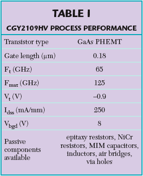
The company has developed a family of advanced GaAs MMIC technologies based on PHEMT and MHEMT structures; the technology used for the CGY2109HV amplifier is the ED02AH 0.18 ?m PHEMT process. This technology is used in applications from fiber optic transimpedance amplifiers, fully integrated core chips to flight qualified components for the space industry. It lends itself ideally to being the main technology for these new ultra low noise, high linearity LNAs. Its performance is shown in Table 1. This high RF performance also translates into an exceptional noise performance with a minimum noise figure of less than 0.1 dB at 900 MHz and only 0.18 dB at 3.5 GHz with a high associated gain.
A Neat Package
Considering the product itself, the CGY2109HV is a dual-LNA MMIC mounted in a plastic 4 × 4 mm QFN 16 pin package. This package is both leadless and has an exposed die pad, making it very suitable for RF applications. It is also available fully RoHS compliant.
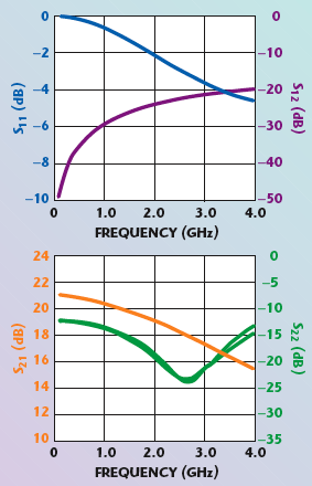
The MMIC mounted in the package is a dual-LNA using the ED02AH process. It has been designed to give both the lowest noise figure and a very high input IP3 with high gain. The measured S-parameters of the CGY2109HV (de-embedded to the pads of the plastic package) are shown in Figure 1. Each graph includes the S-parameters for each of the channels of the dual-LNA and it can be seen that there is negligible difference between the two channels.
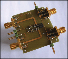
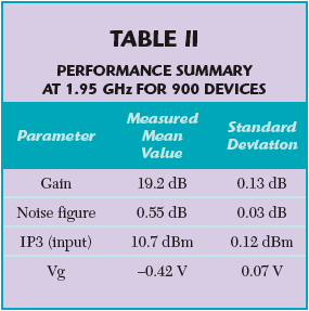
Typically, the new LNA is used with simple input and output matching circuits and is mounted on a low cost substrate such as FR4. The single-ended application board is shown in Figure 2 and the measured performance in Figure 3, with the latter showing the noise figure and gain measured at the board’s connectors (including all the losses due to the connectors and on board matching circuit). At 1.9 GHz a noise figure of 0.5 dB, 19 dB of gain and an input IP3 of 11 dBm is measured with 50 mA per LNA.

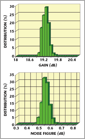
The production test set up was used to measure more than 900 LNAs randomly selected from four wafers from three different production batches. From Figure 4 it can be seen that there is very little variation between adjacent devices as well as very low wafer-to-wafer variations of the noise figure and gain.
The results are summarized in Table 2, where Vg is the gate bias used to establish the required 50 mA drain current. The CGY2109HV can be used either with a constant current or constant gate voltage.
Balanced Configurations
An ideal LNA has a noise figure of 0 dB, perfect input match and generates no intermodulation products. Input match is important especially when a high Q mechanical filter is placed in front of the LNA, which is usually the case in the applications described earlier. Poor input match degrades the filter performance, but achieving a low noise figure and good input match at the same time is frequently contradictory as the GaAs field effect transistors that are usually used for such applications require a different match for low noise figure and low return loss.
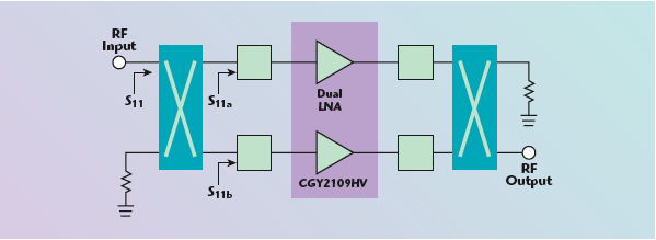
The classic way to circumvent this contradiction is to use a balanced amplifier, as shown in Figure 5. It utilizes two amplifiers of the same type that are placed between two 3 dB hybrid couplers. If the two amplifiers present exactly the same input impedance, all power that is reflected from the amplifiers will be absorbed in the 50 ? load at the fourth port of the input hybrid 90° coupler. In this case the complete amplifier presents a perfect input match even if the two individual amplifiers are not matched to 50 ?.
Under these conditions the input and output match is given by S11 = 1/2(S11a – S11b)
The noise figure will be increased by loss of the coupler but the amplifiers can then be matched for lowest noise figure and not for matching to 50 ?. The overall gain is maintained and the IP3 increased by 3 dB since the input power is divided equally between the two amplifier halves, resulting in the doubling of the power handling compared to using a single amplifier.
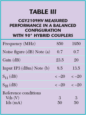
As has been demonstrated, the two LNAs that constitute the CY2109HV are in practice virtually identical, which makes this device an excellent candidate for use in a balanced configuration. The measured performance of the LNA in a balanced configuration with 90° hybrid couplers is given in Table 3. Note that (a) the LNA performance is measured at the connectors of the boards and does not include any de-imbedding of losses on the circuit board itself; and (b) the IP3 is measured with two tones at 1949 and 1951 MHz and with two tones at 849 and 851 MHz.
At 850 MHz a noise figure of 0.7 dB and an output IP3 of 32 dBm is obtained and the input and output return loss is better than –20 dB from 700 to 1100 MHz. At 1950 MHz a noise figure of 0.7 dB and an output IP3 of 33 dBm is obtained and the input and output matching is better than -20 dB from 1.5 to 2.5 GHz.
Yield and Reliability
The constraints in terms of production yield of the base station manufacturer and the long-term reliability of the device are very high. The first requirement is met by the use of a very stable technology with very low component-to-component dispersion and full RF testing (gain, noise figure, IP3) of 100 percent of the plastic-packaged devices.
The reliability of the LNA is achieved through design and the use of a very stable and reliable technology. This high level of long-term reliability has been validated by the use of accelerated aging tests. A total of 147 CGY2109HV coming from different wafers and batches have been subjected to the following tests:
• High temperature storage (150°C) for 1358 hours
• High temperature life testing (150°C) for 1006 hours
• High temperature, high humidity (85°C, 85 percent) for 1680 hours
• Thermal cycling from –55° to +150°C (200 cycles)
No failures were seen during these reliability tests.
Conclusion By combining advanced technology, plastic packaging and careful design, a new product has been developed that is perfectly suited to, amongst others, the base station market. With an amplifier noise figure of 0.5 dB and an output IP3 of 30 dBm, the CGY2109HV is an extremely high performance amplifier.
OMMIC,
Paris, France, 33 1 45 10 67 31,
information@ommic.com,
www.ommic.com