
In the development of high-end electronic devices, a steep rise is being observed in the demand for module solutions for RF components. The reason is to be able to compete in a market that desires new features everyday in the smallest form factor, at lowest current consumption and with best performance. To meet the requirement on the fastest time to market with the right device, the ideal solution for a system designer is to opt for a drop-in module integrating several devices in a single package, without having to go through a long PCB level design cycle and verification. RF front-end design for navigational applications is no exception in this regard.
With the evolution of Global Navigation Satellite System (GNSS) from GPS only into a more complex system, also including Russian GLONASS, European Galileo and Chinese COMPASS, the product development for navigation applications gets challenging. In addition, today's GNSS systems find their application in multi-mode hand-held devices with many other wireless applications co-existing, which can cause interference and jamming. Also, other navigation devices like personal navigation devices (PND), watches, cameras are susceptible to the coupling of high power GSM/UMTS/LTE/WLAN signals, which may interrupt the regular functioning of the device.
First, to achieve state-of-the-art receiver sensitivity levels due to the extremely low signal strengths of GNSS signals, the need for an external low noise amplifier (LNA) is proven to be essential. Due to the ever-growing high power interfering signals, appropriate filters are needed in front of the LNA to suppress these jammers. A pre-filter at the input of the LNA has a dual role in that it prevents the LNA to be driven into saturation by the high power jammer signals and, at the same time, helps achieve a high selectivity for the frequency of interest to enable reception also in worst-case conditions. However, it also adds to the losses of the receiver chain with its insertion loss. So the selection of filter is to be based on an optimum trade-off between insertion loss and rejection levels of out-of-band signals. A post-filter might also be necessary to suppress interfering signals coupling to the system after LNA.

Figure 1 GNSS application diagram.
Infineon, with its expertise in RF technology and design has taken up all the above-stated challenges and successfully designed drop-in front-end solutions for system requirements. Infineon offers three different GNSS RF front-end modules with an integrated pre-filter and LNA. They are optimum for cases where the post-filter is placed close to the GNSS receiver and where the designer has flexibility to choose a post filter of choice (with suitable NF, attenuation, single-ended/balanced). The advantage of using a separate post filter is that the module with pre-filter LNA can be placed close to the antenna to achieve better sensitivity and also enables the use of an additional external active antenna connected directly to the post-filter. All modules feature very low insertion loss/high out-of-band rejection pre-filter, followed by a high performance GNSS LNA (see Figure 1). They are offered in a tiny TSNP-7-10 leadless package (2.3 × 1.7 × 0.73 mm), which makes them the smallest available solutions in the market.
The three product offerings are:
- BGM1033N7: mid-gain version; standard solution to meet high performance GNSS specification.
- BGM1032N7: in addition to BGM1033N7 features, specially designed to suppress LTE Band 13 signals. This LTE band is very critical as the upper frequency of Band 13 is 787 MHz, and the second harmonic of this frequency, that is 1574 MHz, falls exactly into the GPS band.
- BGM1034N7: high gain version; for systems with high losses in the receiver chain. However, the higher gain affects linearity but is still acceptable for applications like PNDs and DSCs, where jamming due to high power cellular signals is less critical.

Figure 2 Performance comparison of BGM 103xN7 series.
The performance of these three modules is shown in Figure 2. Figure 3 shows the in-band gain and out-of-band suppression of the BMG103xN7 series modules, while Figure 4 shows their in-band gain only.
Applications: Smart Phones, Tablet PCs, Personal Navigation Devices (PND), Digital Still Cameras (DSC), Watches, etc.

Figure 3 In-band gain and out-of-band suppression of BGM103xN7 series.
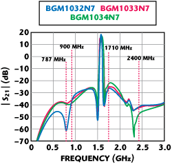
Figure 4 In-band gain of BGM103xN7 series.
Features:
- High Gain: 17.0 dB / 14.8 dB
- Low Noise Figure (GPS): 1.65 dB
- Low current consumption: 4.0 mA / 3.1 mA
- Out-of-band rejection in cellular bands: > 43 dBc
- Input compression point in cellular bands: +30 dBm
- IEC ESD contact discharge of RF input pin in the application: 8 kV
- Supply voltage: 1.5 to 3.6 V
- Tiny TSNP-7-10 leadless package: 2.3 × 1.7 × 0.73 mm
- RF input internally pre-matched
- RF output internally matched to 50 Ω
- RoHS compliant package (Pb-free)
Infineon Technologies AG
Neubiberg, Germany
+49 800 951 951 951
www.infineon.com/gps