
Currently, the defected ground structure (DGS)1-4 has been widely employed to improve filter performance and reduce filter size. DGSs show good stopband performance and excellent harmonic suppression in microwave circuits design and especially the periodic DGSs,4 which extend the stopband greatly. DGS increases the effective capacitance and inductance of a microstrip line and, as a result, restrains the spurious responses by rejecting harmonics in microwave circuits. Consequently, the performance of filters or other microwave components is effectively improved. However, DGS introduces wave leakage through the ground plane.
Compared with a DGS circuit, the typical defected microstrip structure (DMS)5-7 unit is made by etching two vertical narrow slots in the microstrip line, so the enclosure problems need not be considered because there is no leakage through the ground plane. DMS is more easily integrated with other microwave circuits and has an effectively reduced circuit size, compared with DGS. Simultaneously, DMS exhibits the properties of slow-wave, rejecting microwaves at certain frequencies and has an increasing electric length in certain circuits, which are similar to the well known DGS, but without affecting any of the ground plane.
Both DMS and spurline are made with slots on the strip; there is not much difference between the two structures. However, spurline8 commonly refers to the structure shown in Figure 1, and is commonly used to assist a bandpass or bandstop filter design for obtaining better performance. DMS has a more flexible topology, compared with spurline, which can be used in designing filters (including low pass, bandpass and bandstop), power dividers and amplifiers, etc. The defect in microstrip line creates resonance characteristics in the frequency response. Spurline may be regarded as one of the structures of DMS, for both have band rejection performance for certain slot dimensions.
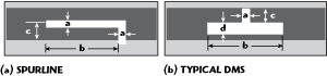
Figure 1 Defected microstrip structures.
In the present work, the defected microstrip structure is studied and novel bandstop filters, with single and dual band, are designed for the first time. Based on EM simulation and similar performance with a DGS, a simple circuit model of a DMS unit is established, and lumped elements are extracted. Two kinds of bandstop filters with a DMS are fabricated and measured, and the experiment confirms the new design.
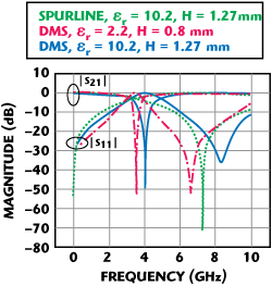
Figure 2 Simulated S-parameters of a 50 Ω microstrip line with DMS and spurline.
Modeling of Defected Microstrip Structure
A DMS consists of a horizontal rectangular slot and a vertical rectangular slot in the middle of conductor strip, as Figure 1 shows. Similar to a DGS, a DMS increases the electric length of microstrip line and disturbs its current distribution, and the effective capacitance and inductance of a microstrip line increase. Accordingly, the DMS has stopband and slow-wave characteristics,1 as shown in Figure 2, for the DMS with εr = 2.2, a = 0.2 mm, b = 13 mm, c = 0.8 mm, d = 1 mm; for the DMS with εr = 10.2, a = 0.2 mm, b = 14 mm, c = 0.3 mm, d = 0.3 mm; for a spurline with εr = 10.2, a = 0.3 mm, b = 8.5 mm, c = 0.6 mm. New microwave components, especially bandstop filters and low pass filters, can be designed by using these characteristics. In order to do a comparison, the simulated results are obtained by using a 50 Ω microstrip line with a substrate relative permittivity of 2.2 and 10.2, and a thickness of 0.8 mm and 1.27 mm, respectively. It can be seen that the spurline and DMS have obvious stopband performance and similar frequency responses, and a bandstop filter can be easily obtained using a substrate with higher permittivity. So, a spurline may be regarded as a kind of defected microstrip structure. In this study, it was observed that the DMS shown can be described by the horizontal slot length b and the vertical slot width a. It shows that the horizontal slot length affects the effective inductance, which increases with b increasing, and introduces a lower stopband. While the vertical slot width affects the effective capacitance, which decreases with a increasing, the lower capacitance induces a higher resonant frequency f0.
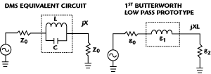
Figure 3 Equivalent circuits of the DMS and Butterworth low pass prototype.
The electrical performance of a stopband with DGS is simulated by a parallel LC resonant circuit.2,5,6 Because the stopband performance of the new DMS is similar to that of the DGS unit, the equivalent circuit model of DGS 2 can be used to extract the equivalent circuit parameters of DMS, as Figure 3 shows, and the equivalent circuit of DMS matches the response of the 1st Butterworth low pass prototype. The reactance of DMS can be expressed as

Where, ω0 denotes the resonant frequency of the parallel LC resonator. The series inductance of the 1st Butterworth low pass prototype shown can be written as

Where, ω' is the normalized angular frequency, Z0 is the characteristic impedance, and g1 is the normalized parameter of the 1st Butterworth low pass prototype. According to circuit theory, the reactance values shown in the figure should be equal when ω = ωc, and the expression is

Here, ωc denotes the cut-off frequency of the parallel LC resonator, and inductance L and capacitance C can be obtained from Equations 1 to 3 as:


The equivalent circuit parameters of the DMS can be calculated from Equation 4, and the calculated values of the lumped-element parameters, using a 50 Ω microstrip line with εr = 2.2 and H = 0.8 mm, are shown in Table 1.

Figure 4 Single band stop filter 1 with DMS.
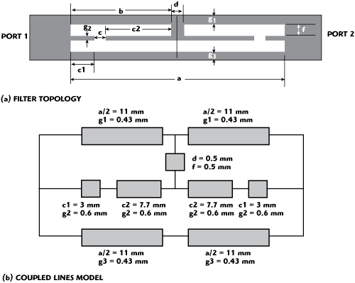
Figure 5 Single band, band stop filter 2 with DMS.

Figure 6 Frequency response of the band stop filter 1 as a function of 1 with c1 = 0.3 m and d = 0.3 mm.

Figure 7 Frequency response of the band stop filter 1 as a function of c1 with d = 0.3 mm and l = 4.4 mm.
Bandstop Filter Designand Experiment
In order to demonstrate the stopband validity of DMS, two kinds of bandstop filters with a single band are designed, as shown in Figures 4 and 5. The coupled lines models of the proposed filters are also shown. For single band bandstop filter 1, designed on a ceramic substrate with relative permittivity of 10.2, and a thickness of 1.27 mm, the simulated frequency responses comparison with topology parameters l, c1 and d are shown in Figures 6, 7 and 8, with a = 0.3 mm, b = 14 mm, respectively. It can be seen that the parameters l, c1 and d have a small influence on filter performances, except for the bandwidth. Simulated filter frequency responses in function of parameter b are shown in Figure 9, where a = 0.2 mm, c1 1 = 0.3 mm, d = 0.3 mm, l = 4.4 mm. It shows the operating frequency increasing with the parameter b decreasing, and for b = 12 mm, the filter has a relative bandwidth of 19.3 percent with a low loss of less than 0.3 dB at the center frequency of 6.75 GHz, and a pair of transmission zeros with an attenuation of more than 39 dB.
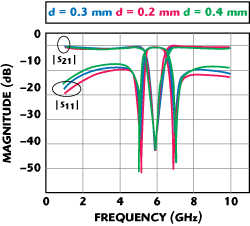
Figure 8 Frequency response of the band stop filter 1 as a function of d with c1 = 0.3 mm and l = 4.4 mm.

Figure 9 Frequency response of the band stop filter 1 as a function of b.
For the single-band bandstop filter 2, which is designed on a duroid substrate with a relative permittivity of 2.2 and a thickness of 0.8 mm, the simulated frequency responses as a function of g2 are shown in Figure 10. It shows the filter center frequency increasing with the parameter g2 decreasing, and a smaller g2 introduces a narrower bandwidth. This kind of DMS also offers a low loss and a pair of transmission zeros.

Figure 10 Simulated frequency response of the band stop filter 2 as a function of g2.

Figure 11 Fabricated band stop filter 2.
In order to verify the design, bandstop filter 2 was fabricated and measured. The circuit size is smaller than 32 × 2.5 mm. The measured results, which are obtained with an Agilent E5071C vector network analyzer, are shown in Figure 11, and are similar to the simulation.

Figure 12 Topology and equivalent circuit of the dual-band band stop filter with DMS.

Figure 13 Simulated frequency response of the dual-band band stop filter as a function of b.
For dual-band bandstop filter implementation, a pair of vertical slots is introduced, as shown in Figure 12. The horizontal slot affects the effective inductance, while the vertical slot affects the effective capacitance. The substrate relative permittivity and thickness of the filter are the same as for the bandstop filter 1. The simulated filter frequency responses as a function of the parameter b are shown in Figure 13, with a = 0.4 mm, c = 1 mm, d = 0.3 mm and e = 0.6 mm. The relationship of the operating frequency with the parameter b is shown in Figure 14. From the two figures, it can be seen that the operating frequencies of the dual-stopband decrease with the horizontal slot length b increasing, and for b = 15.8 mm, the dual-band operate at 1.89 and 5.69 GHz, respectively, and has low loss as well as transmission zeros. When b decreases to 8 mm, a single stopband is introduced. It also shows that the filter has a wide passband between the operating stopband, which is more than twice the filter's first operating frequency and an excellent band-gap performance of DMS is demonstrated.

Figure 14 Relationship of the operating frequency as a function of b.

Figure 15 Fabricated and measured dual-band band stop filter.
The dual-band bandstop filter was fabricated and measured, and the circuit size is less than 30 × 1.2 mm. The measured results shown in Figure 15 are similar to the simulation. The discrepancies between measured and simulated results are mainly due to the simulation precision and fabrication uncertainty.
Conclusion
In this article, a defected microstrip structure is studied, and new bandstop filters with single band and dual band are developed. The measurements demonstrate the new design. Compared with the DGS, the DMS has no enclosure problem because there is no leakage from the ground plane. It shows that the DMS has a flexible design and a controllable operation for bandstop filter implementation, and the new DMS filters have advantages of simple topology, miniature size and better performance of transmission zeros with low loss.
Acknowledgment
This work is supported by Specialized Research Fund for the China Doctoral Program of Higher Education (200805611077), and the Open Research Fund of China State Key Laboratory of Millimeter Waves (K201107), and the Fundamental Research Funds for China Central Universities (2010B22714).
References
- C.S. Kim, J.S. Park, D. Ahn and J.B. Lim, "A Novel 1–D Periodic Defected Ground Structure for Planar Circuits," IEEE Microwave and Guided Wave Letters, Vol. 10, No. 4, April 2000, pp. 131-133.
- D. Ahn, J.S. Park, C.S. Kim, Y. Qian and T. Itoh, "A Design of the Low-pass Filter Using the Novel Microstrip Defected Ground Structure," IEEE Transactions on Microwave Theory and Techniques, Vol. 49, No. 1, January 2001, pp. 86-93.
- J.S. Lim, C.H. Kim, D. Ahn, Y.C. Jeong and S. Nam, "Design of Low-pass Filters Using Defected Grounded Structure," IEEE Transactions on Microwave Theory and Techniques, Vol. 53, No. 8, August 2005, pp. 2539-2555.
- J.K. Xiao, Y.F. Zhu, J.S. Fu, "Non-uniform DGS Low Pass Filter with Ultra-wide Stopband," The 9th International Symposium on Antennas, Propagation and EM Theory (2010 ISAPE), November 30-December 2, 2010, Guangzhou, China.
- S. Zhang, J.K. Xiao, Z.H. Wang and Y. Li, "Novel Low-pass Filters Using Defected Microstrip Structure," Microwave Journal, Vol. 49, No. 9, September 2006, pp. 118-128.
- J.A. Tirado-Mendez and H. Jardon-Aguilar, "Comparison of Defected Ground Structure (DGS) and Defected Microstrip Structure (DMS) Behavior at High Frequencies," 1st International Conference on Electrical and Electronics Engineering Digest (ICEEE), 2004, pp. 7-10.
- J.A. Tirado-Mendez, H. Jardon-Aguilar and F. Iturbide-Sanchez, et al, "A Proposed Defected Microstrip Structure (DMS) Behavior for Reducing Rectangular Patch Antenna Size," Microwave and Optical Technology Letters, Vol. 43, No. 6, 2004, pp. 481-484.
- W.H. Tu and Kai Chang, "Compact Microstrip Bandstop Filter Using Open Stub and Spurline," IEEE Microwave and Wireless Components Letters, Vol. 15, No. 4, 2005, pp. 268-270.