
A diplexer is an essential component in frequency-division duplex (FDD) wireless communication systems. Typical requirements of modern diplexers are compact size, good return loss, low insertion loss and high isolation between two passbands. Packaged diplexers are usually preferred because they can easily be integrated into transceiver subsystems. Therefore, the aim of this work is to present a complete design procedure of packaged microstrip diplexers suitable for commercial off-the-shelf utilization.
In the proposed diplexer, two passbands are centered at 10 and 15 GHz, respectively, and they have an identical bandwidth of 700 MHz. Some trade-offs have to be made between the circuit size and the electrical performance (such as isolation). The circuit size, however, has high priority in this work due to the limited area of the selected package. In the conventional design of diplexers, the two channels of bandpass filters (BPF) are designed independently and subsequently combined at the common input port for achieving the desired duplexing function through iterative optimization. This design scheme would have two shortcomings if the transmitting and receiving passbands have a large frequency separation: one is the large circuit size occupied by two BPFs and the other one is design complexity due to the T-junction at the common input port P1. Its transmission response is frequency-dependent, especially over a wide frequency range, so the T-junction would have to be optimized with great effort so that it would not affect the performance of two channel filters.

Figure 1 Topology simplification from conventional diplexer to SIR-based diplexer.
The concept of stepped-impedance resonator (SIR) was proposed to specially arrange the harmonic frequencies of a transmission line resonator by adjusting its impedance and length ratios.1 Based on this concept, the T-junction and the first resonators in two filtering channels can be replaced by one common SIR,2 of which the fundamental resonance and first harmonic are allocated at two passbands, respectively. This topology simplification is illustrated in Figure 1. As a result, the T-junction is removed and circuit size is greatly reduced. Furthermore, by using dissimilar resonators with staggered harmonic frequency allocations, it is possible to achieve a high rejection of spurious passbands over a wide frequency range.3 In the figure, blue and yellow solid nodes represent resonators of lower and upper bands, respectively, while different patterns indicate dissimilar resonators. Therefore, this work will take full advantage of these special features of SIR in order to develop a compact packaged diplexer with wideband harmonic suppression.

Figure 2 Diagram of the microstrip line diplexer.
Design of the Microstrip Line Diplexer
Figure 2 shows the proposed diplexer combining two BPFs with a common resonator R1. The substrate of choice is RT/duroid® 6010.2LM with a substrate thickness of 0.635 mm and a copper thickness of 17 μm. Half-wavelength SIRs are chosen for all the resonators in order to avoid the use of grounding vias. A three-pole Chebyshev response is selected for both BPFs in order to reach 20 dB attenuation at 10±2 GHz and 15±2 GHz. The 10 GHz BPF is composed of SIRs R1, R2 and R3, while the 15 GHz BPF consists of SIRs R1, R4 and R5.
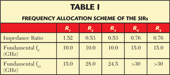
In order to enlarge the stopband, the following frequency allocation scheme is adopted for designing the proposed diplexer. All the results in Table 1 are obtained from full-wave simulations.4 From the table, it is evident that, on one hand, by introducing an impedance ratio larger than 1, the first two resonances of the common resonator R1 are allocated at 10 and 15 GHz, respectively. On the other hand, for all the other resonators (R2 to R5), their first harmonic frequencies are set higher than twice of the fundamental resonant frequency by adjusting their impedance ratios less than 1. Moreover, their harmonic frequencies are staggered, and as a result, spurious passbands can be suppressed over a wide frequency range. However, it should be noted that even when the impedance ratios are the same for R2 and R3 as well as R4 and R5, their first harmonic frequencies are different due to different length ratios of SIRs, as well as different parasitic effects of the microstrip bend or step discontinuities.
According to the design specifications, the following coupling matrices are synthesized for two passbands, respectively.
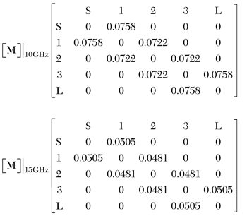
Figure 3 Illustration of the commercial package.
The external quality factor and the coupling coefficients between resonators are subsequently extracted according to the synthesized coupling matrices using the method of Hong and Lancaster.5 In this procedure, attention must be paid to the following two aspects. The first one is that the diplexer should fit into the available area of the selected commercial package.6 Figure 3 shows an illustration of the package. It can be seen that the total dimension of the usable area in the package is only 11.51 × 10.49 mm, or 1.02 λg × 0.93 λg, where λg is the guided wavelength of the 50 Ω line at 10 GHz. The second aspect is the input/output of the diplexer should be located at the exact position of the package leads in order to reduce the parasitic effects of the ribbon bonding. A slight optimization was carried out, based on the initial geometrical dimension, in order to satisfy the design specifications and the final dimensions of the designed diplexer as listed in Table 2 for reference.

Prototyping and Results
Figure 4 shows a perspective view of the packaged diplexer together with the test fixture that is designed using the same substrate. The diplexer is assembled inside the commercial ceramic package with the support of two bonding ribbons on each lead.

Figure 4 Packaged microstrip line diplexer.
Figure 5 Simulation results of the back-to-back transition.

Figure 6 Photograph of the fabricated prototype.
A back-to-back transition between the 50 Ω microstrip line and the package is designed and optimized to achieve a good match between the two passbands. Two stages of impedance transformers are utilized with the second stage meandered for reducing the circuit size. Figure 5 plots the simulated performance of the back-to-back transition, and it shows that the return loss is better than 20 dB for the 10 GHz passband and better than 17 dB for the 15 GHz passband.
After being analyzed in a full-wave simulator, the packaged diplexer together with the test fixture was prototyped and measured with three subminiature version A (SMA) connectors, using a vector network analyzer (Anritsu 37397C). A photograph of the fabricated prototype is given in Figure 6.
The measured scattering parameters are compared with the simulated ones in Figure 7. Good agreement is observed except for the increased insertion loss at the high edge of the 15 GHz passband, which will be discussed below.

Figure 7 Comparison between simulated and measured S-parameters of the packaged diplexer: (a) S12 and S13 (b) S11 and S23.
From figure 7a, it can be seen that in the simulation, the maximum in-band insertion losses are 2.0 and 3.4 dB in the 10 and 15 GHz passbands, respectively. However, the measured maximum insertion losses are 2.5 and 4.8 dB in the 10 and 15 GHz passbands, respectively. The additional loss can be partially ascribed to the insertion loss of the SMA connectors, which is not included in the simulations. Furthermore, if the diplexer is encased, the measured maximum insertion loss in the 15 GHz passband is 4.4 dB, which means there is 0.4 dB radiation loss from the circuit itself.
It is shown in figure 7b that the simulated return loss of the common port P1 is better than 15 dB for both passbands while the measured return loss is better than 14.5 dB in the 10 GHz passband and better than 12.5 dB in the 15 GHz passband. In addition, the simulated isolation is higher than 23.5 dB over the entire frequency band of interest with a measured one better than 22 dB. The isolation can be further improved by allocating transmission zeros in the passband of the other filter.
Finally, the measured group delay, shown in Figure 8, tallies well with the simulated one. Both of them present small in-band variation.
Conclusion

Figure 8 Comparison of group delay between simulation and measurement.
A compact packaged microstrip line diplexer is reported and good results are obtained in both simulation and measurement. This packaged diplexer is very compact and it can be directly and easily applied to wireless communication systems with frequency-division duplex mode.
References
- M. Makimoto and S. Yamashita, "Bandpass Filters Using Parallel Coupled Stripline Stepped Impedance Resonators," IEEE Transactions on Microwave Theory and Techniques, Vol. 28, No. 12, December 1980, pp. 1413-1417.
- C.F. Chen, T.Y. Huang, C.P. Chou and R.B. Wu, "Microstrip Diplexers Design with Common Resonator Sections for Compact Size, but High Isolation," IEEE Transactions on Microwave Theory and Techniques, Vol. 54, No. 5, May 2006, pp. 1945-1952.
- C.F. Chen, T.Y. Huang and R.B. Wu, "Design of Microstrip Bandpass Filters with Multiorder Spurious-mode Suppression," IEEE Transactions on Microwave Theory and Techniques, Vol. 53, No. 12, December 2005, pp. 3788-3793.
- High Frequency Structure Simulator (HFSS). ver. 11.1, Ansoft Corp., Pittsburgh, PA, 2008.
- J.S. Hong and M.J. Lancaster, "Couplings of Microstrip Square Open Loop Resonators for Cross-coupled Planar Microwave Filters," IEEE Transactions on Microwave Theory and Techniques, Vol. 44, No. 11, November 1996, pp. 2099-2109.
- Datasheet of 580450, StratEdge Corp., San Diego, CA, 2009. Available:www.stratedge.com/lcc.htm.