
In tropical regions, satellite communication links at Ku-band frequencies face excess up- and downlink paths loss due to rainfall. The uplink rain attenuation causes a decrease in the signal level received at the satellite receiver, which leads to a decrease of the satellite transmitter power. This signal level is further reduced by the downlink rain attenuation. This may cause the signal level to fall below the sensitivity threshold level of the ground receiver a for specific BER performance. Adaptive power control systems in the satellite transmitter and ground receiver can solve this problem. This article describes the design, development and characterization of a Ku-band channel amplifier with an automatic level control (ALC) system for spacecraft applications to control the input of the final power amplifier (TWTA or SSPA) according to the signal level arriving at the channel amplifier input. Thus, the ALC system also protects the final power amplifier against any accidental high power from the uplink.1 This channel amplifier can operate in an ALC mode as well as in a fixed gain mode (FGM). In the fixed gain mode, the gain is 44 dB and in the ALC mode, the gain varies automatically from 39 to 59 dB depending upon the input power level. This amplifier has an adjustable gain control (22 dB) system to operate the final power amplifier in different back-off conditions in both modes of operation.
The required gain of the amplifier is achieved by using three amplifier modules using PHEMT devices (CFY67-08). In the ALC mode, the channel amplifier operates as a closed loop feedback system.1 The amplifier contains a Schottky diode detector to detect the sampled RF power. This detected voltage is amplified by a differential DC amplifier and applied to the control input of a variable PIN diode attenuator. The attenuation of the attenuator varies according to the input power level so as to maintain the output power level of the channel amplifier constant. Another PIN diode attenuator is used for the adjustable step gain control.
It is known that the gain of the HEMT-based amplifier modules, the attenuation of the PIN diode attenuators and the detected power level of the Schottky diode detector are all functions of temperature. Thus, suitable compensation circuits2–4 are included to compensate for the temperature variation of the channel amplifier’s performance over the required temperature range for satellite applications. A practical systematic procedure based on the measurement data instead of the conventional trial and error method is presented to determine the component values of the compensation networks.
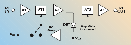
Block Schematic of the Channel Amplifier
The basic block schematic of the channel amplifier with ALC is shown in Figure 1. The amplifier modules A1, A2 and A3 are used to meet the total gain requirement of the channel amplifier. The voltage variable attenuator AT1 is for the automatic gain control of the amplifier, depending on the input power level. The range of gain control of this attenuator is +15 to –5 dB over the nominal gain of 44 dB. The attenuator AT2 is for adjusting the gain of the amplifier by up to –22 dB, in steps of –2 dB. For the ALC function, the RF power is sampled after the amplifier A2 and detected by the detector diode. This detected voltage is applied to one of the inputs of the differential DC amplifier. The other input of the differential amplifier is connected to the reference voltage VR2, which determines the output power level of the channel amplifier. The output of the DC amplifier is connected to the ALC attenuator AT1 through an analog switch. The switch position determines the mode of operation of the channel amplifier. When the switch connects the attenuator AT1 to the other reference voltage VR1, the channel amplifier operates in the fixed gain mode. The voltage VR1 level determines the gain of the channel amplifier in the fixed gain mode operation.
The gain of the microwave amplifier modules, the attenuation of the PIN diode attenuators and the detected power level of the Schottky diode detector are all functions of temperature. Thus, suitable compensation circuits are required to compensate for the temperature variation of the channel amplifier performance over the specified temperature range for satellite transponders.
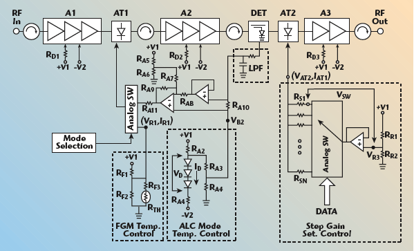
The schematic circuit diagram of the channel amplifier with the different temperature dependent control signals is shown in Figure 2. The temperature-controlled reference voltage VR1 is generated using a thermistor to compensate the gain in FGM operation. The temperature-controlled reference voltage VR2 is generated using P-N junction diodes to compensate the output power level variation in ALC mode operation.1 To achieve a temperature invariant and accurate step attenuation, an improved control circuit is used for the PIN diode attenuator.4
Realization of Individual Modules
Amplifier Modules
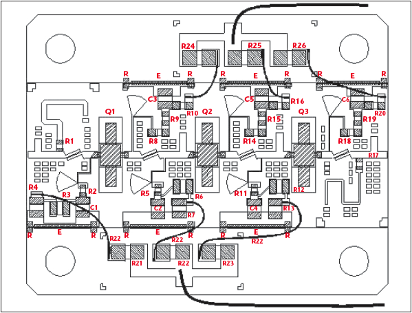
The amplifier modules A1, A2 and A3 are used to achieve the required channel amplifier gain. A1 and A2 are three-stage amplifiers and A3 is a two-stage amplifier. All the amplifier modules are made using PHEMT devices (CFY67-08) for the Ku-band downlink frequency of 11.45 to 11.70 GHz. The MIC assembly drawing of the three-stage amplifier is shown in Figure 3. All the matching networks are fabricated on a 25 mil thick alumina (Al2O3) substrate (?r = 9.9), 0.25" × 0.5", and the required bias resistors are also accommodated on the alumina substrates in the RF tray. The two-stage amplifier A3 is realized with the same MIC cards used in the three-stage amplifier by eliminating one inter-stage matching network. These circuits were simulated and analyzed with the HP (EEsof) circuit simulator, series IV. To adjust the overall gain of the channel amplifier the resistors RD1, RD2 and RD3 are used in the +V1 supply lines of the amplifier A1, A2 and A3, respectively.

Variable Attenuators
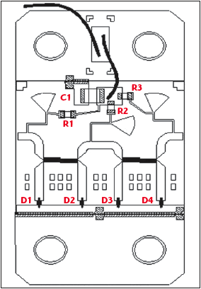
The attenuators for step gain control (22 dB) and automatic level control (20 dB) are both two-stage, PIN diode-based, voltage variable analog attenuators. The MIC assembly drawing of the attenuator is shown in Figure 4. D1, D2, D3 and D4 are beam lead PIN diodes (MPND-4005), connected with 3 dB Lange couplers designed at Ku-band frequencies. In this configuration, the circuit will provide maximum attenuation when the PIN diode resistances are 50 ?, which will be determined by the current through the diode. The photograph of the integrated RF tray is shown in Figure 5.
Temperature Compensation of the Channel Amplifier
It is known that the gain of the PHEMT-based amplifier modules, the attenuation of the PIN diode attenuators and the detected power level of the Schottky diode detector are functions of temperature. Moreover, the temperature dependency of the on-resistance of the analog switch (CD4051) is influenced by the temperature characteristic of the channel amplifier. Thus, suitable temperature compensation circuits, with a suitable method to determine the component values, are required to compensate the temperature variation of the channel amplifier’s performance over the required temperature range for satellite applications. There are two temperature-dependent control signals VR1 and VR2 generated to compensate the temperature variation of the channel amplifier’s gain in the FGM and ALC modes, respectively. Another control signal, VR3, is generated to achieve a temperature invariant step gain setting. The practical procedures to determine the component values of the control circuits for the different modes of operation are discussed in the following sections.
Fixed Gain Mode (FGM)
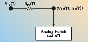
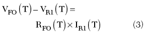
In the fixed gain mode, it must be ensured that the gain of the channel amplifier is within the specified limit over the operating temperature range. The function of the control signal VR1 is to set the gain of the amplifier at 44 dB and to keep this gain within the specified limit (peak-to-peak < 0.8 dB) over the temperature range of –10° to +60°C. To generate the temperature-controlled reference signal VR1, a thermistor RTH is used with the resistors RF1, RF2 and RF3, as shown in the block diagram. The equivalent circuit of the VR1 signal generator with the attenuator and analog switch is shown in Figure 6. Here, the reference point is taken before the analog switch to include its temperature variation. VFO(T) and RFO(T) are function of temperature due to their dependency on RTH(T) and are given by

Suppose that, at a temperature T, the voltage at the reference point and the current to the attenuator is VR1(T) and IR1(T), respectively, to achieve the required gain (44 dB) setting of the channel amplifier. Then from the equivalent circuit
To determine the circuit component values (RF1, RF2 and RF3) of this network, it is required to take three sets of voltage and current readings [{VR1(TA), IR1(TA)}; {VR1(TC), IR(TC)}; VR1(TH), IR1(TH)}] at three different temperatures (TA, TC, TH) by setting the amplifier’s gain at the required value (44 dB). The optimum values of RF1, RF2 and RF3 will be the ones that satisfy Equations 4, 5 and 6 simultaneously

Automatic Level Control Mode
In the ALC mode, the detector circuit will detect the RF power, and there will be a voltage drop across the load resistor RA10. This voltage will be amplified by the differential amplifier and fed to the attenuator AT1 through the analog switch. The reference voltage VR2 will determine the output of the channel amplifier in the ALC mode. The variation of the output power over the range of the input power variation will be determined by the overall gain of the ALC loop. The loop gain is determined by the resistor RA8, RA9, RA10 and RA11. An offset current provided through the resistor RA7 ensures that the output of the differential amplifier is at a negative potential at very low RF power levels. The characteristics of the detector, amplifier modules and attenuators change with temperature. Thus, the reference voltage VR2 should be a temperature dependent voltage to achieve the required fixed output power level within the specified range over the operating temperature range.1 To generate the temperature-controlled reference voltage VR2, P-N junction diodes are used. The following equations determine the current (Id) through the diodes and the voltage (Vd) across all the diodes

Assuming that there is no current drawn by the detector diode and the differential amplifier from the reference supply VR2. Therefore, at a particular temperature T, if the reference voltage requirement is VR2(T), then one can write

The circuit component values (RA1, RA2, RA3 and RA4) of this network can be determined by taking three sets of voltage readings [VR2(TA), VR2(TC), VR2(TH)] at three different temperatures (TA, TC, TH) by setting the amplifier’s output power level at the required value (say 0 dBm). Then the optimum value of RA1, RA2, RA3 and RA4 will be the one which satisfies Equations 10, 11 and 12 simultaneously

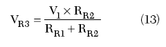
Adjustable Gain Setting
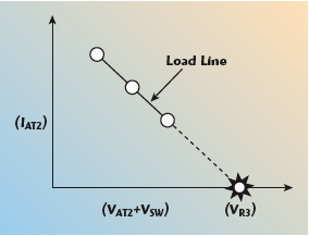
The step attenuator AT2 sets the gain of the channel amplifier. A proper load line selection technique is used to achieve a temperature invariant attenuation of the PIN diode based attenuator AT2.4 An analog switch (CD4051), with a bank of resistors RS1 to RSN and a reference voltage VR3, is used for the control signal of the PIN diode attenuator circuit.4 The reference voltage VR3 is the critical parameter to achieve a temperature invariant attenuation. The resistors RR1 and RR2 determine this reference voltage. To determine RR1 and RR2, three sets of voltage and current readings are required [{VAT2(TA), IAT2(TA), VSW(TA)}; {VAT2(TC), IAT2(TC), VSW(TC)}; {VAT2(TH), IAT2(TH), VSW(TH)}] at three different temperatures (TA, TC, TH) by setting the attenuation of the attenuator, preferably at the maximum required value (say 22 dB). Then, plotting these data as shown in Figure 7, one can get the reference voltage VR3, which is the intercept point of the load line with the voltage (VAT2 + VSW) axis. RR1 and RR2 will then be determined by satisfying the following equation and putting the constraint on current drawn from the source V1
The resistance values RS1 to RSN can be determined by setting the reference voltage VR3 and then adjusting these resistor values to achieve the different step attenuation required (2, 4, 6,… dB). This can be done at any temperature. In this method, the temperature variation of the ‘analog switch resistance’ has been taken into account by plotting the load line with respect to voltage (VAT2 + VSW). Therefore, this procedure eliminates the separate temperature characterization of the ‘analog switch resistance’ over the temperature range.
Test Results
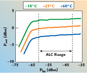
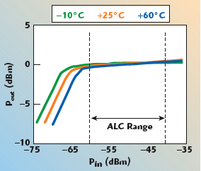
The integrated channel amplifier has been fabricated and tested over the Ku-band downlink frequency of 11.45 to 11.70 GHz. The output versus input power characteristics of the channel amplifier in the ALC mode are shown in Figure 8. The measured output power variation is within 1 dB for an input power variation of –59 to –39 dB. As shown, without the temperature compensation circuit, the output power variation in the ALC mode over the temperature range of –10° to +60°C is nearly 4.5 dB. The required reference voltage (VR2) was measured at cold, ambient and hot temperature to achieve a constant power (0 dBm) at the output of the channel amplifier. The optimum component values RA1, RA2, RA3 and RA4 are determined by satisfying Equations 9, 10 and 11 simultaneously. The power characteristics of the channel amplifier with the optimum components value for the temperature compensation circuit in the ALC mode are shown in Figure 9 at three different temperatures. With the temperature compensation circuit, the measured variation is reduced to less than 0.4 dB over the temperature range of –10° to +60°C.
In the fixed gain mode, without a compensation circuit, the gain variation of the channel amplifier is nearly 5 dB over the temperature range of –10° to +60°C. The three sets of voltage and current readings (VR1, IR1) at cold, ambient and hot temperatures are measured to obtain the same gain of 44 dB. The optimum values of the resistors RF1, RF2, RF3 of the compensation network are determined for a thermistor of 5 k? by satisfying Equations 4, 5 and 6 simultaneously. With the optimum components value of the compensation network, the measured gain variation over the temperature range becomes 0.4 dB. The optimum reference voltage VR3 is determined by the optimum load line selection technique.4 The three sets of voltage and current [(VAT2 + VS), (IAT2)] readings at cold, ambient and hot temperatures are measured to get the same attenuation of 22 dB. Plotting these data, the optimum voltage (VR3) is 0.963 V. For this optimum reference voltage, the resistor values RR1, RR2, and RS1 to RS11 are determined. With this reference voltage, the achieved step attenuation accuracy is within ±0.4 dB for all the steps (–2, –4, ..., –22 dB) over the temperature range of –10° to +60°C.
Conclusion
This article discusses the design, temperature characterization and test results of a Ku-band channel amplifier with an automatic level control (ALC) system for spacecraft applications. The presented practical procedure to determine the component values of the compensation circuits will be very useful to optimize the performance of the channel amplifier without characterizing the individual modules. This systematic procedure takes into account the effect of parameter variation from one unit to another and eliminates the conventional trial and error method, leading to a reduction in labor time.
References
1. S.C. Bera and R.V. Singh, “A Temperature-compensated Closed Loop Overdrive Level Controller for Microwave Solid-state Power Amplifiers,” Microwave Journal, Vol. 47, No. 4, April 2004, pp. 114-122; correction in Microwave Journal, Vol. 47, No. 6, June 2004, p. 156.
2. J.H. Shim, Circuit for Compensating Temperature of Automatic Gain Control Circuit, US Patent No. S 2002/0187766 A1.
3. Wey, et al., Temperature Compensated Variable Attenuator, US Patent No. 6 297 709 B1, 2001.
4. S.C. Bera and P.S. Bharadhwaj, “Insight into PIN Diode Behavior Leads to Improved Control Circuit,” IEEE Transactions on Circuits and Systems-II, Vol. 52, No. 1, January 2005, pp. 1–4.
S.C. Bera received his M. Tech degree in radio physics and electronics from the University of Calcutta, India, in 1994. He joined the Space Applications Center of the Indian Space Research Organization (ISRO), Ahmedabad, India, that same year, where he has been involved in many communication payload projects of ISRO, including the INSAT-2, INSAT-3, INSAT-4 and GSAT series of spacecraft.
R.V. Singh received his B. Tech (EE) degree from GB Pant University of Ag. and Technology, Pantnagar, Nainital, India, in 1972. He joined the Space Applications Center, ISRO, Ahmedabad, India, in October of that year. He has worked on various microwave components and subsystems including low noise amplifiers, receivers and SSPAs for communication satellite transponders. He has worked as associate project director for the communication payload for the INSAT-3A satellite of ISRO. He has contributed to various INSAT- 2, 3 and 4 series communication satellite projects of ISRO. He is presently working as group director of the power amplifier group in the Satcom Payload Technology Area of the Space Applications Center, ISRO.
V.K. Garg received his B. Tech. degree in electronics and communications from IIT, Madras, India, in 1970. He joined the Experimental Satellite Communication Earth Station (ESCES), Ahmedabad, India, in July 1971. Since then, he has been involved in all major communications satellite projects of ISRO, including the SITE, STEP, APPLE, INSAT-1, INSAT-2, INSAT-3 and INSAT-4 series of spacecraft. He was associate project director for the INSAT-2C and INSAT-2D communication payloads. He is currently deputy director, Satcom Payload Technology Area at the Space Applications Center, ISRO, Ahmedabad, India. He is guiding the design and development of regenerative payloads, special payloads and state-of-the-art technology subsystems.