
Radio frequency (RF) interference in a mobile handset has many causes. Closeness of band spectrum, less spatial isolation due to smaller phone size, transmit power and transmitter noise due to filter characteristics are some of the elements that lead to unintentional interference. Because GPS service and cellular carriers exist in most phones, cellular interference affects GPS performance in the following ways:
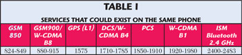
Blocker interference: this type of interference can overload (saturate) the RF front-end of the GPS by driving it into compression. Table 1 shows the services, with their TX frequency bands in MHz that could co-exist with the GPS service on the same phone. Any TX frequency or its harmonic generation with other frequencies could fall in the frequency band of GPS. The front-end filter will not be able to block it because its bandwidth is wide enough to let these types of frequencies go through.
Noise Floor (NF): From the Table, it can be seen that the DCS/W-CDMA B4 are the closest spectrum to the GPS band and therefore represent the major source of TX band noise due to their closeness to the GPS band with non-ideal transmit filter characteristics. The increased noise floor results from the fact that a W-CDMA transmitter is always on in a cell phone, which results in a rise in the noise floor of the total system that will have a one to one effect on the overall sensitivity. Since the GPS signal operates below the thermal noise floor within the given bandwidth, any increase in noise floor (Equation 1) due to out-of-band wideband noise (W-CDMA TX) would result in GPS performance degradation.

The number -174 (in dBm-Hz) is the thermal noise power, which is the kT product of Boltzmann's constant and the absolute temperature in degrees Kelvin in a 1 Hz bandwidth: k = 1.38 × 10⁻²³ J/K, T = 290K.

and -204 dBW = -174 dBm.
2.046 MHz is the typical GPS coarse acquisition (C/A) code bandwidth. The specification for a GPS C/A code signal strength at the GPS antenna is -160 dBW = -130 dBm, well below the noise floor as shown in Figure 1.

Figure 1 GPS signal is below the noise floor (reprinted with permission4).
When pulsed interference penetrates through the front-end within the GPS band, nonlinear gain stages (such as the LNA) could very well be driven into saturation (nonlinear operation). This situation is not desired, because of the fact that not only does the LNA stop providing constant gain, but intermodulation frequency products could be generated and hence provide more sources of interference to the GPS receiver. Depending on how strong the pulsed interference is, the LNA could be so deep in the saturation region that it will take it a longer time to go back and establish the linear operation again. As a consequence, one of the receiver nonlinear subsystem parameters is its recovery time, which is the time it takes the active stage in the receiver to go back to its linear operation after it was driven into saturation by an input power. For example, the recovery time specification of the internal LNA of the SiGe SE4120S GNSS Receiver IC is 1.3 µs, while it is 2 ms for the whole receiver system, based on some criteria such as the input overload signal level for the LNA and the initial value of the rms level of the analog to digital converter for the receiver system.1
Other potential interference sources are the second harmonic input intercept point (IIP2) of the W-CDMA transmitter and the receiver phase noise. The IIP2 frequency could fall within the intermediate frequency bandwidth (IF) of the GPS receiver. Also, the phase noise frequency could mix with the interferer frequency and fall in the IF band.
NF has many sources. One source of contribution is the transmitter's noise, TX noise. The transmitter, which has a power amplifier (PA) as the major component, does not transmit only in the frequency (or bands of frequencies) it is designed for, but it transmits part of its power into other bands (in the form of spurious emissions, due to non-ideal transmit filter characteristics). Based on specifications or measurements, the PA would have tabulated numbers of TX band noise for each band such as GPS or L1 band. For example, 3G B4 (TX frequency: 1710 to 1755 MHz) PA. Its transmit frequency band is 1710 to 1755 MHz at approximately 28 dBm. But the transmitted signal goes through a bandpass filter with a realistic spectrum that does not stop the TX power infinitely at 1710 or 1755 MHz. Instead, part of the power will spill into other bands like GPS band (L1: 1575.42 MHz). As an example, the amount of power that goes into the L1 band, due to a 3G band 2 PA, is -141 dBm/Hz minimum and -138 dBm/Hz maximum.2 This is the amount of noise of a band 2 PA that affects the system noise figure of the GPS receiver. Another example is the 3G B4 PA; -137 dBm/Hz typical and -134 dBm/Hz maximum3 and so on.
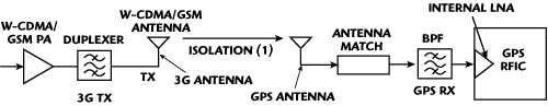
Figure 2 Typical co-existence 3G-GPS scenario.
Another source to the NF is the GPS receiver chain. It is known that each element in the chain has a power loss, which reduces the amount of power (Pin) that goes into the element to a power out (Pout). The total loss across the chain translates into a noise figure. Figure 2 depicts a general representation of a 3G TX system and a GPS RX system.
Analysis and Background
In the following, the background and analysis behind some of NF sources is presented.
NF Due to GPS RX System Hardware
The GPS RX hardware is made up of a chain of components and transmission lines (starting with the antenna match) that will have insertion loss and/or mismatch loss between two consecutive matching stages. By looking at the figure, let us denote the GPS RX filter (BPF is actually called Blocker filter) insertion loss as IL1. Let us denote the total noise figure of the RFIC as NF. The NF for the RX system, without the effect of 3G TX, is RX_NF (excluding the antenna and antenna match):

As an example, typical numbers for IL1 is 1 dB and NF = 2 dB. First, all the dB numbers have to be converted to ratios. Then, RX_NF = 10 log (2) = 3 dB
3G TX Power and Noise Contribution to NF
3G maximum TX power is usually specified at the antenna connector to be 24 dBm; let us denote the maximum TX power by PWTX. The antenna to antenna isolation is denoted as I. The antenna to antenna isolation figure includes the gains/losses of both the 3G TX system and GPS RX system antennas, respectively. Denote the noise of the 3G TX into the GPS band as NWTX. Then the NF due to TX noise into the GPS band (NFTXNoise) is calculated as follows:

where RX_NF is the receive noise figure, as shown above, a denotes the duplexer attenuation. In most 3G PA modules, the specified TX power includes the effect of the duplexer. Then a = 0. As an example, typical numbers for PWTX is 24 dBm, NWTX = -190 dBc/Hz, I = 15 dB and RX_NF = 3 dB, then NFTXNoise = 10log (1+10(174+ 24 -190-15-0- 3)/10)) = 0.41 dB
Based on the above two examples, the total noise figure (NF) of the whole system (due to TX band noise + RX_NF):Total NF = 3 + 0.41 = 3.41 dB
A typical number for a total NF, due to 3G TX noise and hardware chain, into L1 Band is 4 to 5 dB of NF, embodied in a rise in noise floor of the GPS RX system. That means the desired signal is 4 to 5 dB lower than the noise floor. That would be a dB-for-dB of sensitivity degradation. The effect of raising the noise floor reflects on the tracking capability of the GPS receiver.
NF Due to Mismatch Loss (Return Loss)
Another source of NF is the mismatch loss. This is due to impedance mismatch between the source of the signal and the destination. These are usually assessed through measurements and/or simulations and then incorporated into the system NF equation. This could be incorporated in Equation 3 as well.

Figure 3 Current GPS RFICs have a built-in internal LNA.
This discussion assumes a 50 Ω input impedance into the RF input of the RFIC. Usually, the RF input of the RFIC is the input impedance of the internal LNA of the RFIC, which changes based on its bias point conditions. This input impedance is seldom a 50 Ω system. Instead, most of the time, it falls way down in the capacitive region of the Smith chart, as shown in Figure 3. On the other hand, a BPF is a 50 Ω input and output system. This dictates a matching circuit between the output of BPF (50 Ω in and out) and the input of the RFIC and the existence of a mismatch loss (ML), due to reflection. When the reflection is converted to dB, it is called return loss (RL).
In this case Equation 3 needs to incorporate the effect of ML:


Figure 4 GPS receiver possible front-end.
Mitigation Techniques
The above analysis shows that once the 3G transmitter is on, there is no way of suppressing its noise effect, unless a 3G PA is designed that has very stringent requirements on its TX noise NWTX into the GPS band; say -200 dB/Hz, and reduce the 3G power PWTX to a lower level, say 15 dBm, whenever an unsatisfactory level of sensitivity degradation is detected due to 3G TX noise. A third way is to reduce the RF front-end system noise figure by adding an LNA in the lineup, as shown in Figure 4. Based on the architecture and analysis shown and Equation 6, there is approximately 2.5 dB of improvement due to adding the LNA in the front-end lineup.

Conclusion
The above analysis and results show that if a mobile handset product is chosen to offer both GPS and 3G services at the same time to its customers, design decisions have to be made and sacrifices have to be made. These sacrifices could be based on performance or cost. If loss of GPS service or sensitivity degradation is acceptable during a 3G call, then one might want the cheaper solution with no LNA in the lineup. If, on other hand, one would like to maintain a 3G call along with a better GPS performance, then one might want to make a cost and complexity decision, by adding the LNA in the front-end lineup. But the LNA is not the only component added. Its associated bias circuitry, matching circuitry and another bandpass filter in the lineup are needed in addition to dealing with board layout headaches to make sure the LNA is stable and performing to system level specifications. GPS performance, these days, is extremely important, where in some situations it is a safety issue. It should be mentioned, however, that other techniques such as pulse blanking offer a suboptimal solution to mitigate pulse interference.5 Blanking does not only suppress the interfering pulse signal but also suppresses the desired GPS signal for the duration of the pulse. In some designs, pulse blanking leads to approximately 1 to 3 dB in signal to noise ratio degradation.
References
- SiGe Semiconductor, "SE4120S GNSS Receiver IC," 2008.
- Avago Technologies, "UMTS Band2 (1850 to 1910 MHz) 4×4 mm Power Amplifier Module," Datasheet, 2009.
- Avago Technologies, "UTMS1700/2100(1710 to 1755 MHz) and UMTS1700 (1750 to 1785 MHz)," Datasheet, 2009.
- K. Borre, D.M. Akos, N. Bertelsen, P. Rinder and S.H. Jensen, A Software Defined GPS and Galileo Receiver, Birkhauser Boston, MA, 2007, p. 66.
- C. Hegarty, A.J. Van Dierendonck, D. Bobyn, M. Tran, T. Kim and J. Grabowski, "Suppression of Pulsed Interference Through Blanking," Proceedings of the IAIN World Congress, June 26-28, 2000, San Diego, CA.
Appendix: Measurement Procedure
Figure A1 shows an outline of the proposed measurement procedure and equipment needed.

Figure A1 Proposed measurement procedure and equipment.
Apparatus needed:
1) A PC controlling the GPS device. 2) USB connection. 3) Any device with GPS service. 4) A GPS antenna. 5) A 3G transmit source. 6) A tunable notch filter that stops the fundamental. This filter will act as the selectivity of the GPS antenna. It should be set to approximately 40 dB of rejection. 7) A combiner that combines the GPS (desired) signal and 3G (Jammer) signal and feeds them into the input port SMA connector of the GPS device. 8) RF cables and connectors.
Procedure (see Figure A1):
- The PC controls the GPS simulator to run at a certain power level.
- The GSM/W-CDMA transmit source will transmit signal at the lowest channel (W-CDMA B4: Chan 1312 to 1712.4 MHz).
- The fundamental in 2 gets attenuated by approximately 40 dB represented by the notch filter so it does not overload the front-end of the receiver.
- The signals from 1 and 3 are combined using a power combiner.
- The signal out of the combiner goes in the GPS SMA pig tail coax.
There is a 15 dB of isolation representing spatial isolation, I, b/w the GSM/W-CDMA antenna and the GPS antenna.

Figure A2 Impact of W-CDMA TX band 4 noise on the GPS receiver sensitivity.
Results:
The results are shown in Figure A2 for the case of 3G TX set to W-CDMA band 4 (W-CDMA B4) with the following observations:
Plot colors:
- The purple color is the theoretical (ideal) sensitivity (one-to-one); no losses whatsoever. This is without the presence of NF due to line up insertion loss (IL) or mismatch loss (ML).
- The blue color is sensitivity characterization, no W-CDMA TX noise. This is only due to hardware lineup.
- The orange color is sensitivity characterization due to TX Band 4 noise and hardware lineup.
- The green color is with external LNA place in the front-end lineup-equation (6).
- The GPS receiver stopped tracking satellites at input power levels of -156 dBm and lower.
- Worst case in loss of sensitivity is approximately 5.4 dB at -156 dBm of input power, which agrees with the sample calculations made. In other words, due to the presence of W-CDMA TX noise, the sensitivity of the GPS receiver dropped approximately 2.5 dB.
- One can use typical numbers of their system lineup in the equations above that would correlate with their measurements.
Taher AlSharabati is a faculty member at Al-Ahlyah Amman University–Amman, Jordan, and a PhD student at the University of South Carolina, Columbia, SC. He obtained his BSEE degree at St. Cloud State University, St. Cloud, MN, and his MSEE degree at the University of Toledo, Toledo, OH. He has many years of industry experience with almost eight years at Motorola Inc.
Yinchao Chen currently is with the Department of Electrical Engineering, University of South Carolina as an Associate Professor. His current research interests include signal integrity for high speed circuits; computational electromagnetics; RF, millimeter-wave and microwave integrated circuits; wireless communication devices; electronic packaging modeling for VLSI devices; and antenna and scattering applications. Chen has published over 200 international publications. He is a co-author of the book, Multiresolution Time Domain Scheme for Electromagnetic Engineering, a contributor of nine book chapters, and a co-editor of two books.