
Recently, in order to achieve highly efficient amplification, switch mode power amplifiers (SMPA) with theoretical 100 percent efficiency have been introduced. However, in practice, the efficiency of SMPA cannot achieve as high as 100 percent because of the parasitic parameters of the transistor, the losses of matching networks, etc. Among the subclasses of SMPA, inverse Class F has the highest drain efficiency, due to shaping the drain voltage waveform as half-sinusoidal and the drain current waveform as a square-wave.1-2 Many successful design instances of inverse Class F PA have been reported.3-6
Modern and next generation wireless communication systems require high data rate and high spectrum utilization. In this case, the orthogonal frequency division multiplexing (OFDM) signal with high peak-to-average power ratio (PAPR) are being used. Although the inverse Class F PA obtains high efficiency at peak power level, the high PAPR causes low efficiency at the average output power. And the higher the PAPR is, the lower the efficiency will be. Therefore, a crest factor reduction (CFR) technique7-8 is employed to reduce the PAPR so as to enhance the efficiency of the PA.
In this article, a 2.5 to 2.6 GHz inverse Class F PA is implemented using Cree’s CGH40010 GaN HEMT for linear amplification in OFDM systems. The input and output harmonic matching networks (HMN) are analytically designed to make the harmonic impedances approximate the values obtained by harmonic source/load pull simulations. CW measurement shows a greater than 75 percent drain efficiency at 2.55 GHz. For a 20 MHz four-carrier OFDM signal with PAPR of 10.39 dB, after employing CFR and digital predistortion (DPD) techniques, the inverse Class F PA achieves good linearity and 31.9 percent efficiency at an average output power of 34.3 dBm.
Inverse Class F Design Procedure
Inverse Class F Operation and GaN HEMT
Ideally, an infinite number of even-harmonic resonators results in an inverse Class F mode with a half-sinusoidal voltage waveform and a square current waveform at the device output terminal.9 However, it is impractical to control an infinite number of harmonics using microstrip transmission lines. In this design, only the second and third harmonics are considered. The maximally flat drain voltage and current expressions of inverse Class F PA with the second harmonic open loaded and the third harmonic short loaded are shown below:10
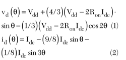
where Vdd and Idc are the drain DC supply voltage and current, Ron is the switching on-resistance of the transistor.
According to Equations 1 and 2, setting Vdd = 28 V, Idc = 0.6 A and Ron = 0.5 , the peak drain voltage value for inverse Class F equals to 73.7 V, which is much greater than the peak drain voltage value 55.2 V for Class F operation under the same condition. This results in a higher efficiency of inverse Class F than its Class F counterpart.
GaN HEMT’s large material band gap permits it to operate at high drain voltage and high power density.11 For Cree’s CGH40010, the maximum drain to source voltage is 84 V,12 which is large enough for inverse Class F operation with a peak drain voltage of 73.7 V. While for Freescale’s LDMOS FET (such as MRF7S35015), the maximum drain to source voltage is 65 V,13 which could not meet the requirement of inverse Class F operation. In this case, a GaN HEMT becomes a promising candidate for inverse Class F PA design.
Load Pull/Source Pull Simulation Steps
- With the large signal transistor model of CGH40010 provided by Cree, load pull and source pull simulations are carried out in Agilent’s Advanced Design System (ADS). The center frequency is set at 2.55 GHz, and the transistor is biased at Vgs = -3.6 V and Vds = 28 V with an input power level of 26 dBm. The objective of the simulation is to find out the optimum load and source impedances at both the fundamental frequency and harmonics, when the power-added efficiency (PAE) is maximum, with a high output power. The simulation is performed through the following steps: Set the fundamental source impedance at a default value to perform fundamental load pull simulation, the optimum fundamental load impedance ZL_fund is obtained. Perform fundamental source pull simulation with ZL_fund to get the optimum fundamental source impedance ZS_fund. Several iterations are needed before the optimum fundamental impedances converge. After convergence, ZS_fund = (6.4-j4) Ω and ZL_fund = (13.21+j16.906) Ω are obtained.
- Perform inverse Class F harmonic load pull simulation with ZS_fund and ZL_fund. In this simulation, only the second and third harmonics are considered and the values of the harmonic impedances are restricted to be purely reactive for the successive design. After simulation, the optimum second harmonic load impedance ZL_2nd = j844.097Ω and the optimum third harmonic load impedance ZL_3rd = -j5.987 Ω are obtained.
- Perform harmonic source pull simulation. From simulation results, the third harmonic source impedance has little effect on the PAE, while the second harmonic source impedance affects it a lot. The optimum second harmonic source impedance is obtained as ZS_2nd = -j27.968 Ω. The PAE simulation results obtained by varying the second harmonic source impedance are shown in Figure 1. Without any losses, the maximum possible PAE could be 83 percent, when ZS_2nd = -j27.968 Ω. If the second harmonic source impedance is not well controlled in the design, the PAE would drop to 67 percent, a considerable decrease of 16 percent. The input HMN helps to provide a second harmonic source impedance as close as possible to ZS_2nd.
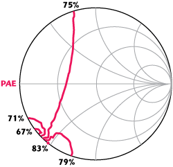
Figure 1 Harmonic source pull simulation.

Figure 2 Schematic of the designed inverse Class F PA.
HMN Analytical Design and Schematic Simulation
Figure 2 shows the circuit schematic of the proposed inverse Class F PA. The input/output HMN controls the harmonic source/load impedances for the values obtained by harmonic source/load pull simulation. The input/output fundamental matching network (FMN) then transforms the fundamental impedances Z*’S/Z*’L to 50 Ω. The analytical design procedure for both HMNs is described as follows.
In the output HMN, the electrical length θ4 and θ6 of the two open stubs are set at π/4 and π/6, which provide a short-circuit at the two junctions for the second and third harmonics, respectively. For the second harmonic load impedance, Equations 3 and 4 can be obtained:

By solving the equation ZL(2f0) = ZL_2nd = j844.097 Ω, when Z3 = 50 Ω, one gets θ3 = 43.3°. The value of Z3 can be altered according to the width of the transistor’s drain pad.
For the third harmonic load impedance, one gets:
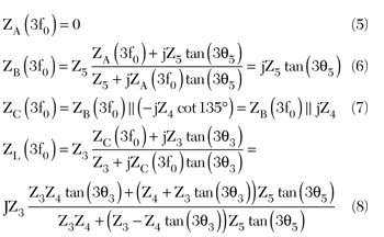
By solving the equation ZL(3f0) = ZL_3rd = -j5.987 Ω, when Z4 = 50 Ω and Z5 = 50 Ω, one gets θ5 = 28.9°. The parameters of the output HMN are now determined. According to the same principle, the parameters of the input HMN can be determined.
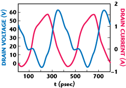
Figure 3 Simulated drain voltage and current waveforms.
Figure 3 shows the simulated drain voltage and current waveforms of the proposed inverse Class F PA. It can be observed that the two waveforms are distorted, when compared with the ideal waveforms of inverse Class F operation. This is because the effects of the nonlinear parasitic parameters that exist in the transistor package. If the package is de-embedded and the waveforms are simulated at the intrinsic drain, the results would be closer to the ideal condition.
From the schematic harmonic balance (HB) simulation in ADS, the maximum in-band PAE of 84.2 percent is obtained at 2.55 GHz, with an output power of 39.54 dBm and a transducer power gain of 13.54 dB.
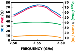
Figure 4 Measured amplifier performance.
Measurement and Linearization
A 2.5 to 2.6 GHz inverse Class F PA has been fabricated to validate the design approach. The selected substrate is RF-35 from Taconic Co. with a dielectric constant of 3.5 and a thickness of 30 mil.
CW Signal Measurement
By setting Vgs = -3.6 V and Vds = 28 V with a 26 dBm input power, the measured PAE, drain efficiency (DE), output power and power gain are plotted in Figure 4 within the frequency band from 2.5 to 2.6 GHz. DE is greater than 52 percent, PAE is greater than 47.7 percent and the output power is greater than 36.9 dBm within the 100 MHz bandwidth. The peak DE of 75.2 percent and peak PAE of 73 percent are observed at 2.55 GHz with a maximum output power and power gain of 41.43 and 15.43 dB, respectively.
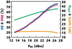
Figure 5 Measured results vs. input power.
Driven by a 2.55 GHz CW input signal with the power swept from 13 to 27 dBm, the measurement results of the inverse Class F PA are plotted in Figure 5 with Vgs = -3.6 V, Vds = 28 V. When the input power reaches 27 dBm, the DE and PAE are 76 and 73.5 percent, respectively. However, the power gain has been compressed to 14.6 dB, a 2.2 dB compression, compared with the maximum power gain observed at a 20 dBm input power.
In Figure 6, the drain to source voltage is varied from 20 to 29 V, with the input power fixed at 26 dBm and Vgs = -3.6 V. DE and PAE achieve a maximum of 79 and 75.4 percent, respectively, at Vds = 21 V.
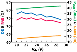
Figure 6 Measured results vs. drain to source voltage.
Linearization with Digital Predistortion
The PA DPD linearization system consists of a vector signal generator (Rohde & Schwarz SMBV100A), a vector signal analyzer (Agilent VSA-E4445A), a PC with Matlab and Agilent’s 89600 and the proposed inverse Class F GaN PA. The SMBV100A, E4445A and PC are connected via a local area network (LAN). The configuration of the system is shown in Figure 7.
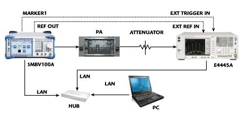
Figure 7 The PA DPD linearization system configuration.
The baseband I/Q signals are modulated and up-converted to an RF signal in SMBV100A, the RF signal is then amplified and distorted by the PA. After attenuation, the RF output signal of the PA is down-converted and demodulated by E4445A. Finally, the output I/Q samples are collected in VSA 89600 for modeling. Using the Hammerstein architecture,14 the inverse PA model (digital predistorter) can be established with the input and output I/Q samples of the PA. With the digital predistorter, the distortion of the PA can be compensated.
The input signal of the PA is chosen as a four-carrier OFDM QPSK signal with a 20 MHz bandwidth and 10.39 dB PAPR at the 0.01 percent level of the complementary cumulative distribution function (CCDF). After CFR with a soft clipping technique,8 the PAPR is decreased to 8.05 dB.
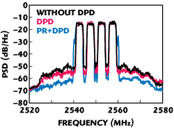
Figure 8 Measured PSD before and after linearization.
Figure 8 shows the measured four-carrier OFDM PSD of the PA before and after linearization. The black trace indicates the original output of the PA. The adjacent channel leakage ratio (ACLR) is -37.48 dBc (lower) and -36.94 dBc (upper) at an average output power of 34.3 dBm. After DPD with Hammerstein, the output PSD of the PA is shown by the red trace, the ACLR of which is suppressed to -41 dBc (lower) and -39.38 dBc (upper). A slight improvement is achieved at this power level of the inverse Class F PA. When the baseband I/Q signal is processed by CFR, distorted by the digital predistorter, and then downloaded to SMBV100A as the input signal of the PA, the output PSD of the PA is shown by the blue trace, the ACLR of which is equal to -48.22 dBc (lower) and -45.8 dBc (upper). The efficiency of the PA is 31.9 percent at a 34.3 dBm average output power.
Conclusion
This article presented an analytical design approach of inverse Class F PA. The input and output HMNs controlled the source and load harmonic impedances appropriately. The fabricated 2.5 to 2.6 GHz GaN inverse Class F PA achieved a maximum in band drain efficiency greater than 75 percent, with an output power of 41.4 dBm at 2.55 GHz. For linearization, the PAPR of the 20 MHz four-carrier OFDM signal was reduced from 10.39 dB to 8.05 dB through a CFR technique. Then, by using DPD, based on Hammerstein, the ACLR was improved to less than -45 dBc at an average output power of 34.3 dBm with 31.9 percent efficiency. According to the experimental results, the proposed inverse Class F PA is suitable for linear amplification with high efficiency.
Acknowledgment
This work was supported by the National Key Technologies R&D Program of China under Grant 2010ZX03007-003-02 and in part by the National High-Tech Project under Grant 2009AA011801.
References
- C.J. Wei, P. DiCarlo, Y.A. Tkachenko, R. McMorrow and D. Bartle, “Analysis and Experimental Waveform Study on Inverse Class F Mode of Microwave Power FETs,” 2000 IEEE MTT-S International Microwave Symposium Digest, pp. 525-528.
- Y.Y. Woo, Y. Yang and B. Kim, “Analysis and Experiments for High-efficiency Class F and Inverse Class F Power Amplifiers,” IEEE Transactions on Microwave Theory and Techniques, Vol. 54, No. 5, May 2006, pp. 1969-1974.
- D.Y.T. Wu and S. Boumaiza, “10 W GaN Inverse Class F PA with Input/Output Harmonic Termination for High Efficiency WiMAX Transmitter,” IEEE 10th Annual Wireless and Microwave Technology Conference Digest, April 2009, pp. 1-4.
- A. Al Tanany, A. Sayed and G. Boeck, “Design of Class F-1 Power Amplifier Using GaN pHEMT for Industrial Applications,” German Microwave Conference Digest, March 2009, pp. 1-4.
- A. Grebennikov, “High-efficiency Transmission-line GaN HEMT Inverse Class F Power Amplifier for Active Antenna Arrays,” 2009 Asia Pacific Microwave Conference Digest, pp. 317-320.
- P. Saad, H.M. Nemati, M. Thorsell, K. Andersson and C. Fager, “An Inverse Class F GaN HEMT Power Amplifier with 78 Percent PAE at 3.5 GHz,” 2009 European Microwave Conference Digest, pp. 496-499.
- S.H. Han and J.H. Lee, “An Overview of Peak-to-average Power Ratio Reduction Techniques for Multicarrier Transmission,” IEEE Wireless Communications, Vol. 12, No. 2, April 2005, pp. 56–65.
- O. Väänänen, J. Vankka and K. Halonen, “Simple Algorithm for Peak Windowing and Its Application in GSM, EDGE and W-CDMA Systems,” IEEE Proceedings, Communications, Vol. 152, No. 3, 2005, pp. 357-362.
- A. Grebennikov and N.O. Sokal, Switch-mode RF Power Amplifiers, Elsevier, Burlington, MA, 2007.
- Y. Xu, J. Wang and X. Zhu, “Analysis and Implementation of Inverse Class F Power Amplifier for 3.5 GHz Transmitters,” 2010 Asia-Pacific Microwave Conference Proceedings.
- Aethercomm, “Gallium Nitride Microwave Transistor Technology for Radar Applications,” Microwave Journal, Vol. 51, No. 1, January 2008, pp. 106-114.
- Technical Data, CGH40010, Cree, available: www.cree.com/products/pdf/ CGH40010.pdf.
- Technical Data, Document Number: MRF7S35015HS, Freescale Semiconductor, available: http://cache.freescale.com/files/rf_if/doc/data_sheet/MRF7S35015HS.pdf.
- J. Zhai, J. Zhou, L. Zhang, J. Zhao and W. Hong, “Dynamic Behavioral Modeling of Power Amplifiers Using ANFIS-based Hammerstein,” IEEE Microwaves and Wireless Components Letters, Vol. 18, No. 10, October 2008, pp. 704-706.