
The next generation of wireless applications requires tunable or reconfigurable components to realize multifunctional RF systems. In current broadband RF systems, filtering dominates size and cost.1,2 These filters are not tunable and hence limit the usable frequency range of most RF front-ends. An alternative to the use of static filters located before or after the power amplifier is a reconfigurable PA, which can be difficult to design for high performance. A multiband PA with narrow bandwidth was achieved by employing a tunable T-section or π-section interstage matching network whose structure is a bandpass filter. These topologies transform the impedances to intersect with high Q-factor contours on the Smith chart, resulting in narrower bandwidth.3
Integrating the tunable impedance matching network into the interstage of the amplifier has several advantages. The rapid impedance variation provided by the first and second amplifier stages results in a narrow bandwidth. The resistance in the lower-Q tuning inductors also helps to stabilize the second amplifier stage. Exploitation of interstage mismatch loss is used for gain equalization to compensate for the gain roll-off of the active devices used in stages 1 and 2. The reflections in the interstage are acceptable because they allow the input and output of the amplifier to be conjugately matched. Also, by including the tunable matching network into the interstage of the PA, the resulting switch and inductor losses do not affect the input noise figure or output power of the amplifier. Finally, when multiband operation is required, a reconfigurable amplifier requires less die space than many single-band amplifiers typically used in the conventional approach.
A CMOS PA, described in the literature,4 also uses the interstage for tuning purposes. However, each tuning state has a broad bandwidth and considerable gain fluctuation. In an earlier work,3 a reconfigurable power amplifier with a tunable interstage matching network was realized by using a two-stage MMIC PA and discrete components for the interstage matching network. The devices are placed on a three-layer prototype board with 50 Ω lines with dimensions of 4 cm × 5 cm. The MMIC PA is located at the center of the board and 25.4 μm diameter gold wire bonds are used to connect the bond pads on the die to the board microstrip line runners. The input and output matching networks were kept fixed while the switching function of the interstage matching network was implemented using a Skyworks AS204 SP4T switch.
At higher frequencies, the size of discrete components becomes large compared to the wavelength and the surface-mount components (SMT) can self-resonate or the parasitic effects begin to dominate. Electromagnetic coupling and parasitic effects from the prototype board become more evident, which cause difficulties in the design process. Therefore, the results from the earlier discrete design suggest that a MMIC implementation of the tunable interstage matching network becomes necessary for higher frequency operation.3 This is due to fewer parasitics being present and better control over component values in the MMIC implementation.
In this article, a reconfigurable power amplifier fabricated using three MMICs is described. The two-stage PA occupies a single MMIC die and the tunable interstage matching network occupies two MMIC die. GaAs FETs are used in the design to provide the switching function instead of varactor diodes or MEMS switches. Varactor diodes have limited linearity and low power handling capability, while MEMS switches are high cost and require a high DC supply voltage. These components cannot be realized monolithically and lead to larger circuit size and higher cost. Therefore, GaAs FETs are used to perform switching in the interstage matching network.
MMIC Design Methodology
The reconfigurable PA, including the MMIC tuner design, can be used for applications covering GSM, CDMA, Bluetooth and WiMAX for frequencies from 0.9 to 2.4 GHz. Circuit design and DC analysis were performed using the Agilent Advanced Design System (ADS).

Figure 1 Simplified schematic of the interstage matching network.
Circuit Design andSmall-signal Performance
The first step in the design is the selection of the first- and second-stage BJTs, including biasing and ballast networks, and input and output matching for 1 to 2 GHz operation. This initial design uses simple high-pass and low-pass L-section matching networks for the input and output. A blocking capacitor is used in the interstage and some resistive loading is used to improve stability. The output impedance of the first-stage amplifier (Z1) and the input impedance of the second-stage amplifier (Z2) were then calculated. Figure 1 shows the π-section impedance matching network used in the interstage. This network has a bandpass response. Impedance matching using a Smith chart was used to determine the initial components values.
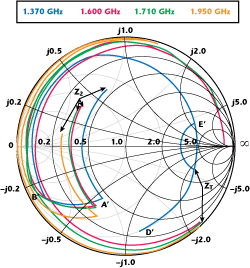
Figure 2 Impedance matching transformation using a Smith chart.
Figure 2 shows the impedance transformations used to reach the high-Q contour on the Smith chart. The series capacitor C4 transforms the input impedance of the second-stage amplifier, Z2 to A’. The shunt capacitor C3 then transforms A’ to B’, the series inductor L2 transforms B’ to C’, the shunt capacitor C2 transforms C’ to D’, the shunt inductor L1 transforms D’ to E’ and finally the series capacitor C1 transforms E’ to ZT. Ideally, to ensure maximum power transfer through the network, the impedance should be transformed from Z2 to the exact conjugate match Z1*. However, the transformed impedance is ZT, whose difference from Z1* results in mismatch loss that is exploited to equalize the gain between the states.
Transformation to the high resistance region of the Smith chart (E’) is also necessary for minimum bandwidth.5 In addition to the transformation purpose, the series capacitors (C1 and C4) also behave as DC blocking capacitors. The shunt capacitor C2 is realized by using four shunt capacitors with FET switches placed in series for frequency control. Here, the center frequency switching takes place by varying the capacitance value and thus changing the mismatch loss in the interstage.
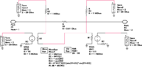
Figure 3 Schematic diagram of M-probe for implementation in ADS.
Mismatch loss in the interstage matching network was calculated using the mismatch probe or M-probe. Figure 3 shows the schematic diagram of the M-probe used with ADS, which is adapted from the S-probe tool.6 The M-probe is a non-invasive analysis that can be placed at an arbitrary point within the circuit.7 The M-probe uses Equation 1 to compute the mismatch loss or mismatch factor between two complex impedances Z1 = R1 + jX1 and Z2 = R2 + jX2.8


Figure 4 Interstage mismatch loss.
Since M-probe is non-invasive, it is easy to implement and can be computed quickly. It is particularly useful in circuit design, where only a specific part of a large circuit is analyzed, that is the interstage. Figure 4 shows a plot of the interstage mismatch loss calculated at the input to the interstage of the amplifier for four different FET switch states. The interstage mismatch loss has a response that is bandpass and decreases monotonically with increasing tuning frequency.

The mismatch loss in the interstage for each tuning state is tabulated in Table 1. The circuit was designed with higher mismatch loss at lower frequency since the gain of the two amplifier stages rolls off with increasing frequency. Therefore, the gain roll-off from stages 1 and 2 are compensated or equalized by this mismatch loss.
In the initial design, the decrease in S21 over the design bandwidth was approximately 4 dB. After obtaining the initial component values using the Smith Chart, the interstage was re-tuned and analyzed for flat amplifier gain (S21) response using the M-probe. Finally, the input and output matching networks for the PA were tuned to provide for wideband low input and output return losses. In the final design, the measured gain (S21) variation was only ± 0.7 dB.

Figure 5 Detailed schematic diagram of a GaAs MMIC reconfigurable PA.
A detailed schematic diagram of the final reconfigurable MMIC power amplifier using tunable interstage matching network is shown in Figure 5. This shows the two-stage amplifier, fixed input and output matching network, tunable interstage matching network and the DC biasing network.
DC Analysis
The circuit is biased using the input bias Vin = 1.4 V (Iin = 1.32 mA), output1 bias Vout1 = 3.6 V (Iout1 = 25.4 mA) and output2 bias Vout2 = 3.6 V (Iout2 = 137 mA), which are required to operate the two-stage amplifier. Series RF chokes and shunt bypass capacitors are placed between each DC power supply and the circuit to provide adequate isolation between each of the amplifier stages. The center frequency tuning is performed by changing the control voltage of the four FET switches (V1, V2, V3 and V4) for turn on or off. Changing the FET switch state varies the overall shunt capacitance value (C2). To limit the current flow into each FET switch, a 1.96 kΩ resistor is placed in series with each gate terminal and control line.
The DC bias networks included RF chokes and bypass capacitors to provide isolation between the amplifier stages and improve the stability. Broadband stability analysis was performed on each amplifier stage and also at each tuning state to ensure unconditional stability. Rollet’s condition, where K > 1 and |Δ| < 1, is satisfied to achieve stability.8
Fabrication
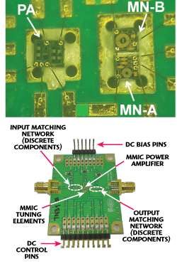
Figure 6 Fabricated prototype of the reconfigurable power amplifier.
Figure 6 shows the fabricated prototype of the reconfigurable power amplifier, including the two-stage power amplifier and the tunable interstage matching network and the prototype board. The MMIC PA and MMIC tuner were fabricated on three different die and co-located on the prototype board. The die shown on the left side is a two-stage power amplifier (PA) having dimensions of 720 μm × 660 μm and the two tuner die shown on the right side are 600 μm × 600 μm (MN-A and MN-B). These die are the tunable interstage matching network that provides center frequency tuning function. Separate die for the tuner were necessary because of limited wafer space. The input and output matching networks were fixed and realized using surface-mount components (0402 and 0805 SMT). For the low tuning bandwidth (35 percent), the optimum load impedance for maximum power transfer is assumed to be independent of frequency.
The three-layer prototype board has dimensions of 4 cm × 5 cm and 50 Ω microstrip lines. The top DC pins are used to supply the DC bias to operate the two-stage amplifier and the bottom DC pins are used to switch the control voltages (V1, V2, V3 and V4).
Simulation and Measurements

The circuit simulation was performed using the Agilent Advanced Design System (ADS) and the effects of parasitics from the prototype board were modeled using Sonnet™. The SMT S-parameter data that are available from the vendors were also included in the circuit simulation. A sensitivity analysis was used to consider any effects due to possible variations in the prototype board on the circuit performance. The length and width of the microstrip lines in the circuit simulations were varied to ensure that any effects due to these variations were minimal.
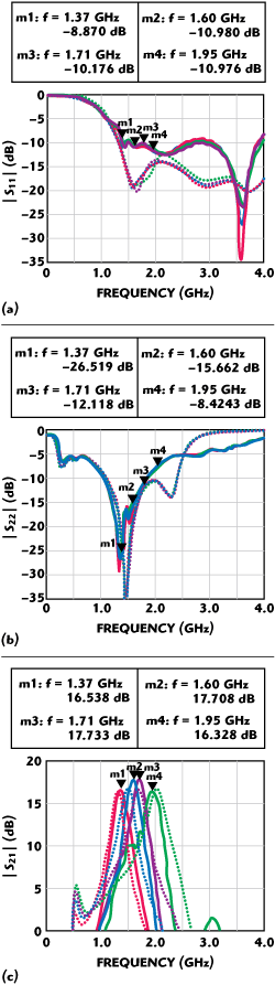
Figure 7 Measured and simulated S-parameters of the GaAs MMIC reconfigurable power amplifier.
Small-signal Measurement
The small-signal response of the reconfigurable MMIC PA was simulated and measured. An Agilent E5071C Network Analyzer was used to measure the S-parameters. Table 2 shows the combination of FET switch tuning states and the total shunt capacitance value used to tune the center frequencies to 1.37, 1.60, 1.71 and 1.95 GHz.
Figure 7 shows the measured (solid lines) and simulated (dotted lines) S21, S11 and S22, at four different center frequencies. The fabricated prototype shows 17 dB (± 0.7 dB) measured gain and gives reasonable agreement with the simulated gain. The measured input reflection coefficient (S11) is less than -10 dB at most of the operating frequencies. The output reflection coefficient (S22) varies between -8.5 and -26.5 dB for the different switch states. The minimum reverse isolation (S12) is -50 dB for all states.
Table 3 shows the measured 3 dB bandwidth at each operating frequency and its corresponding Q-factor. The Q-factor is nearly constant for all tuning states. The measured 3 dB bandwidth varied from 260 to 320 MHz between the tuning states.

Large-signal Measurement
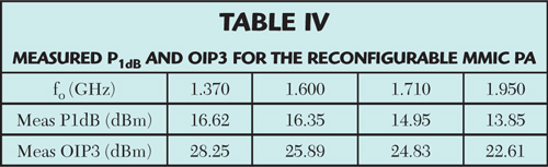
The Agilent MXA N9020A Spectrum Analyzer and Agilent MXG N5181A Analog Signal Generator were used to measure the large-signal power performance. OIP3 and P1dB for each state were measured at the corresponding operating frequency (fo) and are tabulated in Table 4. The maximum measured OIP3 and P1dB at 1.370 GHz are 28.25 and 16.62 dBm, respectively.
Conclusion
This article presents the design methodology for a reconfigurable power amplifier with a tunable interstage matching network. The fabricated prototype operates at center frequencies between 1.37 to 1.95 GHz, which cover several standards of digital telephony. The reconfigurable PA was fabricated using 3 MMIC die and a test board. The measured gain (S21) of the reconfigurable amplifier is 17 dB (± 0.7 dB) over the tuning bandwidth. Future work includes the development of an integrated MMIC including the power amplifier and tuning elements onto a single die to achieve a broader tuning range and higher frequency of operation.
References
- M.B. Steer and W.D. Palmer, Multi-functional Adaptive Microwave Circuits and Systems, Scitech Publishing, 2009.
- E.D. Adler, et al., “Special Issue on Multifunctional RF Systems: Guest Editorial,” IEEE Transactions on Microwave Theory and Techniques, Vol. 53, No. 3, Part 2, March 2005, pp. 1005-1008.
- R. Gani, G.A. Ellis and C.S. Teoh, “Reconfigurable MMIC Power Amplifier Using a Discrete Interstage Matching Network,” 2009 IEEE International Conference on Antennas, Propagation and Systems (INAS) Proceedings, December 2009.
- S.O. Yun and H.J. Yoo, “A Reconfigurable CMOS Power Amplifier with Flexible Matching Network,” 2006 Asia Pacific Microwave Conference Proceedings, pp. 512-515.
- L. Besser and R. Gilmore, Practical RF Circuit Design for Modern Wireless Systems, Vol. 1: Passive Circuits and Systems, Artech House, Norwood, MA, 2003, pp. 262-264.
- K. Wang, M. Jones and S. Nelson, “The S-probe: A New, Cost-effective, 4-gamma Method for Evaluating Multi-stage Amplifier Stability,” 1992 IEEE MTT-S International Microwave Symposium Digest, Vol. 2, pp. 829-832.
- G.A. Ellis, “A Novel Technique for the Analysis and Optimization of Interstage Networks in Microwave Power Amplifier Design,” EAB 4523 – Microwave Devices and Circuits Course Notes, Universiti Teknologi Petronas.
- G. Gonzalez, Microwave Transistor Amplifiers: Analysis and Design, Second Edition, Prentice Hall, London, UK, 1997.
Regina Gani received her BEng and MSc degrees in electrical and electronic engineering from Universiti Teknologi Petronas, Perak, Malaysia, in 2008 and 2010, respectively. Her research interests include RF integrated design (RFIC), MMIC design and reconfigurable microwave devices.
Grant A. Ellis received his PhD degree in electrical engineering from the University of Washington at Seattle in 1995. He is currently professor of electrical and electronic engineering at the Universiti Teknologi Petronas in Tronoh, Malaysia. His current research interests include monolithic microwave integrated circuit (MMIC) and RFIC design, novel millimeter-wave MMIC design, microwave computer aided design techniques and electrically small antennas.
Teoh Chin Soon received his BEng degree in electronic engineering and his PhD degree in microwave engineering from the University of Manchester, UK, in 1992 and 1996, respectively. From 1996 to 1997, he was with SCM Integrated Systems in Kuala Lumpur. Subsequently he joined the Test and Measurement Division of Hewlett-Packard in 1997 (now Agilent Technologies) as an application engineer for RF/MW and wireless instrumentation and later on developed and supported test solutions for mobile wireless handsets. In 2002 he moved into RFIC design work with Avago Technologies. In early 2007, he founded DreamCore Technologies Sdn Bhd to provide RF design services to the electronics industry. In the past three years, he has designed and developed many GaAs/InGaP RFICs such as low-noise amplifiers, power amplifiers and RF switches, as well as RF test boards and fixtures for customers in Malaysia, the US and China.