
More than ever, linearization schemes for radio frequency (RF) power amplifiers (PA) have become a necessity. Modern PAs are facing ever-increasing challenges in terms of power efficiency (PE) and performance requirements. Solutions relying heavily on digital signal processing are mature and readily available today, but are not without their drawbacks. Besides, new standards, markets and applications are creating new challenges that these state-of-the-art techniques called digital predistortion (DPD) are not always able to solve.
One of the most exemplar challenges for DPD is the linearization of low power PAs that can be found in multi-antenna arrays or femtocell applications. For those applications, relying on a 5 to10 W DPD system to linearize a 5 W PA, for instance, does not make much sense.
With the need for alternative and simpler linearization methods, one needs to take an orthogonal approach, or what is called the analog approach. Analog predistortion (APD) faces unusual design challenges, even for the seasoned designer. First and foremost, textbooks do not cover it in much detail. The simplest questions arise but stay unanswered: How do you model the system? What do you need to specify? How do you perform simulation? How does a circuit specification translate into system performance?
While the most common analog blocks such as phase-locked loops, mixers or bandgap voltage references have been extensively analyzed and reported, little can be found on analog signal processing, or on analog computing building blocks. This article describes the peculiar aspects of APD in terms of requirements and provides a few pointers on the analog techniques of choice to implement an analog linearizer.
The PA and Its Need for Linearization
Among the PA parameters, designers must fulfill three that are all equally important and difficult to meet at the same time. Other equally important parameters, such as gain, have less relevance to PD techniques and are therefore not mentioned in this article. The first goal is to transfer all the electrical energy from the power plug into RF energy that will be radiated through the air. The ratio of the RF energy to the consumed power is power efficiency.
The second goal, which is intimately related to the first, is the linearity. It defines the quality of the signal that will be transmitted and also the amount of interferences generated into neighboring channels. For the present purpose, linearity can be defined as a metric that measures the quality of the signal after being distorted by an amplifier.
The last goal is the video bandwidth (VBW). In a nutshell, higher VBW means more users and higher data rates from the end user’s favorite smartphone.
While the first cellular standards like GSM were created to simply make phone calls, modern standards like 3G and 4G have been primarily developed to handle greater data transmission and ultimately give users access to new services such as video streaming. The shift to those modern air interfaces has changed the PA requirements quite substantially. W-CMDA, for instance, calls for VBWs that are at least ten times greater than GSM. Worse, in order for a 3G-PA to be properly linearized, its VBW should be even greater because the linearizer will expand the signal, as will be discussed later in this article.
Predistortion’s Principle and Implementation
Principle
Predistortion (PD) is basically a way of improving the linearity of the PA. Why is that a good thing? Because linearity can be traded for power efficiency. A good PD system allows the PA designer to make the PA less linear but more efficient, knowing that the lost linearity can be recovered by the linearizer. The PD principle is extremely simple and has given its name to the technique. The idea is to preprocess, or predistort, the signal applied to the PA, rather that trying to improve the PA itself.

Figure 1 PA distortion.
Figure 1 shows this principle. On the left-hand side, the red signal is the input applied to the PA. The blue curve shows the output of the PA. Where a straight line following the red line is expected, one can see that as the signal becomes larger, the amplifier is not able to follow the input anymore; it is compressing. On the right-hand side, the input signal is predistorted (cyan) and the output of the PA (green) is now a straight line; the PA is said to be more linear. It is interesting to note that while the blue line was pointing down, the green line is pointing up; it is expanding.
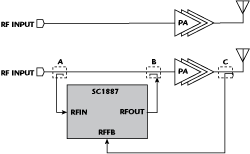
Figure 2 Predistorter (SC 1887) application schematic.
Implementation
Following the predistortion principle, the actual implementation of an analog PD solution is very straightforward and can be hooked up in a few minutes to any existing PA. Figure 2 illustrates the simplicity of such a system. The RF input signal RFIN is connected to the analog predistorter’s input, called RFIN (coupler A). The predistorted signal coming out of RFOUT is added (coupler B) to RFIN at the input of the PA. A last signal called RFFB (coupler C) is used to analyze the output of the PA and adapt the predistortion signal. It should be noted that unlike in a digital PD system, all of the inputs and outputs are RF/analog signals. Among other things, this makes it independent of protocol. Any adaptive PD system, analog or digital, requires two main subsystems: an analyzing and processing engine and a correction engine.

Figure 3 Error measurement.
Analyzing and Processing Engine
The first thing that needs to be done is analyzing the signal to extract metrics that describe the quality of the incoming signals RFIN and RFFB. These metrics are called cost functions (CF). RFIN is the signal sent by the transceiver to the input of the PA. As such, this signal has the highest spectral purity, that is free of distortion and only limited in quality by the transmitter baseband and upconverter. RFFB is basically the output of the PA, only attenuated to accommodate the power levels at the input of the linearizer. This signal is strongly distorted by the PA. It is the signal that must be improved. Having these two inputs allows a few operations, such as subtracting them to obtain the error introduced by the PA (see Figure 3).
It is also possible to take a look at RFFB and measure its spectral purity by measuring the energy in the band of interest and out of the band. Figure 4 shows the measured adjacent channel leakage ratio (ACLR) output of a PA for a single-carrier W-CDMA signal.

Figure 4 In-band vs. out-of-band.

Figure 5 Polynomial generation.
Correction Path
The correction block is the heart of the system. Its role is to apply mathematical transformations to the incoming RF signal. These transformations are called the work function (WF). The work function is an approximation of the PA’s inverse transfer function. Ideally, the predistorting transformation is cancelled out by the amplifier’s distorting transformation, resulting in an undistorted, amplified output signal. Due to the nonlinear behavior of the PA, its inverse function can be approximated by a polynomial function; the higher the order of the polynomial, the better the approximation of the mathematical transformation. Figure 5 demonstrates a possible implementation of such a polynomial. The input signal X is passed through a number of multipliers to generate its harmonics: X, X2, …, Xn. Those harmonics are then multiplied by a series of coefficients c1, c2,…, cn and finally summed together to create a polynomial of the form: c1X + c2X2 +…+ cnXn.

Figure 6 Memory effect.
In DPD, these operations are realized in the digital domain. Analog predistortion is using analog multipliers and digital-to-analog-converters (DAC) for the coefficients.
One fundamental mechanism of the PA is the so-called memory effect. In a nutshell, the PA transfer function is not constant over time and will vary. In other words, the output of the PA depends on its input at all times. Figure 6 shows how the PA characteristic is affected by the memory effect; its output spreads.
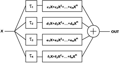
Figure 7 Memory compensation.
To accommodate for these memory effects, the polynomial has to be replaced with a set of polynomials (see Figure 7). Each of the polynomials is identical, but is fed by a time shifted version of the input signal X. Such a mathematical representation is called a Volterra Series and was developed by Vito Volterra in 1887. The analog predistorter contains four memory terms. Each of them is made of a programmable delay, followed by a 6th order polynomial.

Figure 8 Adaptation algorithm.
Adaptation Related Issues
The system must be continuously adaptive to compensate for changes. It basically learns from its mistakes and becomes better over time. When the device starts, it waits for an input signal and then goes through an adaptation loop (see Figure 8). When the adaptation is over after a few seconds, the device will go into power saving, but will keep looking at the incoming signal regularly and immediately go back to adaptation if necessary.
The adaptation principle is quite simple. Starting with some random coefficients, a few sets of random coefficients are applied and the result measured. Out of these trials, the best coefficients are selected, and the loop is repeated until the linearity target is reached.
This algorithm, while being robust and simple, puts a high burden on the analog blocks on the chip. When the device enters the ‘sleep state’, the on-chip temperature drops by a few tens of degrees Celsius. These temperature changes are happening many times per second and should have no impact on the analog path in order for the PD signal to stay constant.
Also, during adaptation, the algorithm applies random coefficients on the online signal, the signal sent to the PA. If too much of the perturbation energy is applied, the PA linearity will degrade and violate the spectrum requirement. On the other hand, if the applied perturbation is too small, the cost function will not change significantly enough to be meaningful, hence useful for adaptation. In order for this mechanism to work, the gain settings throughout the chip have to be tightly controlled over process, voltage and temperature (PVT). Only a tight control will ensure that the perturbation energy is controlled.
Design Issues Explained
Bandwidth Expansion
Predistortion is all about signal expansion, hence bandwidth expansion. For a given input signal at a frequency f0, the PA will generate distortion products at multiples of this frequency: 2f0, 3f0, 4f0, 5f0, 6f0, 7f0, etc. While this is a good thing for a rock guitar, modern telecommunication PA spectral output requirements are very stringent and do not tolerate too much distortion. The higher order harmonics’ energy is high enough to significantly degrade the spectrum up to the 7th order.
This means the linearizer should be able to generate frequencies at least up to 7f0 to cancel this distortion product at the output of the PA. In other words, for a 40 MHz VBW input signal, the linearizer should have a 280 MHz VBW. This also implies that the PA has a VBW high enough to allow the correction signal to be passed to its output.

Figure 9 Compression vs. expansion.
Square-cube Law Factor Dilemma
While being extremely simple, the square-cube law has dramatic consequences on all physics phenomena. This law teaches that certain forces will matter more or less depending on the magnitude of a particular physics quantity. What does this all have to do with the topic? Take a 1 V sinusoid and square it. This would be the simplest way to generate the second harmonic of the signal. The output signal will be 1 V (see Figure 9). Now, do the same thing with a 10 and 0.1 V signal. The outputs will be 100 and 10 m V, respectively. In the first case, the output of the multiplier expanded — 100 V > 1 V — and in the second, the signal has been severely compressed — 10 mV < 0.1 V.
What this means is that for ‘larger’ input signals, the polynomial generator output will be rapidly overwhelmed while smaller signals will virtually vanish. Solutions to the expansion are two-fold: increasing the dynamic range and increasing the resolution of the coefficient DACs. The compression issue can only be resolved by amplifying the signal, that is adding gain. A high gain can be achieved using a cascade of amplification stages with the drawback that each stage requires power and adds noise. Low noise amplification is therefore a must.
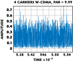
Figure 10 Peak to average ratio.
Peak-to-Average Ratio Burden
The peak-to-average ratio (PAR) is the ratio between the peak of the signal and its average. In Figure 10, a short time sample of a four carrier W-CDMA signal with a 10 dB PAR is shown. A single peak above 0.7 can be seen, while most of the signal (the average) is much lower. Multicarrier applications, modern standards and OFDM, in particular, lead to very high PAR. What is important to understand from a design standpoint is that the analog circuits within the linearizer basically have the same problem as the PA. They have to support a high dynamic range to accommodate the PAR. Worse, because the linearizer has to create high order correction terms for the polynomial, it will actually expand the PAR. Table 1 demonstrates this expansion for a 10 dB PAR signal.

As can be seen, when the order of the signal increases, the average signal drops at a very fast pacebecause each time the input signal is squared, the output is an order of magnitude smaller than the input. In order to compensate for these losses, at least 20 dB gain must be added after each squaring function.
Circuit Limitations and Considerations
Linearity of the MOS Device
With all its advantages, the MOS transistor is not a very linear device; its well-known square law V-I relationship limits its usability where linear transconductance stages are needed. In other words, independent of the load or type of circuit used, one cannot apply a 1 V signal at its gate and expect 60 dB linearity at its output; 10 to 20 dB is all one will get.
The most widely used techniques to overcome this limitation are to use the transistor in a closed-loop circuit. Closing the loop reduces the input signal seen by the transistor to a few tens of a mV, while keeping a large output signal and ultimately improving its linearity. As everything in life, however, this does not come for free. Closed-loop circuits are relying on feedback to work and feedback always comes too late. Given BW and gain requirements, applying feedback would have been difficult, and perhaps even impossible. To rely exclusively on open-loop circuitry was preferred.
Process, Voltage and Temperature Variation Impact
Dealing with process, voltage and temperature variations is the essence of an analog designer’s job. Process variations come from the imperfect manufacturing of silicon structures. The outcome is that the devices that are fabricated will vary from wafer to wafer.

Voltage variation can be mostly handled by architecture choice and has little impact on most of the important design parameters other than power consumption. Temperature, on the other hand, is a real beast. The characteristics of a transistor on a chip will change a lot with temperature. The gain of an analog multiplier can easily change by a factor of 2.5 (8 dB) between -40° and 125°C (industrial temperature range). For reference, Table 2 shows how the temperature affects the harmonics’ amplitude coming out of the polynomial generator. As can be seen, the signal amplitude after subsequent multiplications will vary greatly. Further, non-idealities will actually make the situation even worse.
A Few Answers
Design Partitioning
Proper design partitioning is key to such a complex analog processing architecture. The wrong partitioning can quickly lead to losses such as signal degradation, high power consumption, linearity degradation, and high noise figure or bandwidth degradation. Also, while certain design techniques can be applied in exceptional cases, their implementation is often heavy in terms of real estate, complexity or power consumption, and is therefore not suitable for circuits like multipliers and DACs that need to be replicated tens of times on a chip.
- A few simple rules can be used as a guide through the architecture choices and tradeoffs:
Combine functions:- Amplification should never be made stand-alone but be part of another function
- And its corollary: the signal should not be attenuated without good reason
- Amplification should never be made stand-alone but be part of another function
- Use passive circuits as much as possible
- Minimize the hardware
- Limit the number of active stages
- Control all the circuit parameters
- Make the physical design (layout) part of the design process
- Reuse building blocks and/or make them scalable
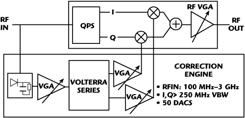
Figure 11 Signal Path.
Implementation of the Analog Signal Processing Path
Figure 11 depicts a simplified version of an implementation of the analog signal path. The RF signal is fed to the RF signal processor (RFSP) and to the correction engine (CORR). The signal path can handle RF frequencies going from 700 MHz to 3 GHz.

Figure 12 Current summing1.
RFSP’s first stage is a quadrature phase shifter (QPS). It is an analog polyphase filter, whose purpose is to extract the in-phase (I) and quadrature (Q) signals; having I and Q signals allows one to change both the phase and amplitude of RFIN. I and Q are multiplied by the corresponding I/Q signals generated by CORR. The outputs of the multipliers are then added together and connected to RFOUT. RF VGA acts as a driver and a voltage-controlled amplifier for finer control over the correction signal.
CORR is mostly a baseband analog processor. The first stage brings the RF signal down to baseband by extracting its envelope. The output is then buffered through another VGA that drives the Volterra series generator that was described previously. It actually generates two series to correct I and Q independently. The VGAs were added at the interface, instead of plain drivers, to gain flexibility and granularity.

Figure 13 Current summing2.

Figure 14 Current summing1Current summing with amplification.
Current Mode Approach
When it comes to summing and amplifying signals at high speed, current mode clearly outperforms voltage. Summing signals is as easy as connecting two nodes together, as shown in Figures 12 and 13. Great amplification can be achieved by using a simple resistor. However, when isolation and impedance transformation are required, a transimpedance amplifier (TIA) will do the job nicely (see Figure 14). High gain can be achieved by increasing the resistance of feedback resistors. For example, for i1 = i2 = 50 μA and R = 1 kΩ, Vout = 100 mV.

Figure 15 Replica biasing.
Replica Biasing
As was seen before, it is critical to control the gain of the circuits over PVT. It was also concluded that it was not possible to use closed-loop circuits to do so, mainly because of the BW requirements. A common way of regulating parameters over PVT is to use what is called replica biasing. Replica biasing consists of making a perfect copy (see Figure 15) of an active circuit. This replica is then included in a regulation loop that will control a specific parameter of this circuit. The output signal of the control loop V regulator is connected to both replica and active circuits. The replica circuit is using copies of the devices gm and R. In this case, it is forcing the equation: gmR = 0.
Replica circuits are not new and are far from perfect. First, they are additional circuitry that serve no functional purpose. They take real estate and consume power. The achievable accuracy is therefore limited.
The outlined approach makes extensive use of replica biasing to control every single circuit in the CORR path. However, one particularity is that while different replicas are used, the same control circuit is employed everywhere.
Conclusion
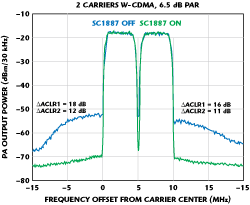
Figure 16 Two carriers W-CDMA.
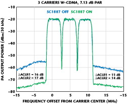
Figure 17 Three carriers W-CDMA.
Figures 16 and 17 show typical measurements taken with an implementation in standard CMOS of some of the techniques described and a Doherty PA for W-CDMA waveforms. The center frequency is 2.19 GHz. This demonstrates that analog predistortion can be successfully used for PA linearization. Complex GHz signal processing can be done in the analog domain by carefully selecting the architecture and design techniques. While being a new technology, it is also very robust. This design is scalable and flexible and can be easily adapted to other applications.