
The coaxial to rectangular waveguide transition is one of the most important devices used in microwave and millimeter-wave circuits. Especially at millimeter-waves, a waveguide-to-coaxial adapter is one of the most often used components for efficient electromagnetic wave transmission and high power handling. Although many types of adapters are available commercially for frequency below 15 GHz, not many of them with simple structures and easy integration with other circuits have been reported for millimeter-waves. For instance, one of the 8 mm waveguide-to-coax adapters provided by Wiltron is reported to have a VSWR ≤ 1.25 in the frequency range of 26.6 to 40 GHz. However, the device needs additional attached fixtures, such as a tuning screw or pin, without which the performance is poor. Figure 1 shows the simulation model and the calculated VSWR of the adapter without the tuning screw. It can be seen that the VSWR changes dramatically within the frequency band and is generally larger than four. In other words, the performance of the device is sensitive to, or very much dependent on, the tuning screws and pin. It not only presents challenges in the design and fabrication process, but also makes the adapter difficult to integrate with other circuit structures such as active integrated antennas.

Figure 1 (a) Simulation model of a common waveguide to coax adapter structure and (b) simulated VSWR of the adapter without tuning screws.
Moreover, quite a number of challenges still remain for the design. For instance, little improvement has been made to extend the adapter’s bandwidth without sacrificing the performance. A relatively larger transverse electromagnetic wave loss still exists due to the control of the characteristics of the dielectric used to support the inner conductor. In addition, to carry out the impedance match between a waveguide to a coaxial line (that is from 377 to 50 Ω) has not always been easy within a compact volume. Investigations along this line have been reported in the literature.1-5
In order to circumvent the above problems, a new concept needs to be developed. In this article, a novel structure for an 8 mm coaxial to rectangular waveguide transition in Ka-band is presented that can be easily integrated with antenna waveguide feeding circuit structures. A periodic, two-dimensional photonic band gap (PBG) structure is applied to a dielectric in the coaxial line to mitigate the transverse electromagnetic wave loss, and a step impedance structure is used to realize an efficient energy transmission. Numerical simulations were performed on the proposed structure to show the performance obtained. Experiments have been conducted to validate the new design.
The Proposed Structure and Its Design
PBG structures have recently gained great attention in both theoretical studies and practical applications. They are periodical structures that are designed to affect electromagnetic wave propagation in the same way as the periodic electrostatic potentials in a crystal structure affect the electron motion, by defining allowed and forbidden (the gap) electronic energy bands. Such structures create the possibility of effective manipulations of electromagnetic wave emission and propagation processes.
Periodic structures for electromagnetic waves were proposed during the early days of microwave radars. Photonic band gap (PBG) structures are one type of the typical periodic structures. They originated from the work of E. Yablonovitch at UCLA, where one-dimensional periodic slots were cut along a metallic waveguide. Later, they were extended to one-, two- and three-dimensions and are generally known as the “Electromagnetic Band Gap (EBG)” structures. Electrically, they form a type of structure that prevents the propagation of the electromagnetic waves in a specified band of frequency. The main factors affecting the characteristics of PBG have been found to be the number of periodic units, the geometry configuration, dimensions, array mode and dielectric constants.2, 5-8

Figure 2 Circular dielectric column in a PBG structure.
There are two types of two-dimensional (2D) PBG dielectric column structures: solid column and vacuum column array (see Figure 2). In the present case, the latter has been chosen and applied to the dielectric of the coaxial line. Its use not only improves the electrical performance, but also provides support for the inner conductor. More specifically, these vacuum columns help reduce transverse wave loss and serve electrically as a filter, while mechanically it still works as a support. The conducting loss will not be increased because the PBG is constructed in the dielectric support, where the electromagnetic field density is still concentrated around the inner conductor.
In the implementation, a double layer 2D PBG configuration was adopted. Given the specifications, the thickness and period of the PBG structure can be computed by using electromagnetic simulators; the central cut-off frequency can be estimated with the following classical formula

where c is the speed of light in vacuum, β stands for the propagation constant in the dielectric, β0 is the propagation constant in vacuum, a is the period of PBG and fstop is the central cut-off frequency.
In the present case, the central pass band frequency is f0 = 37.5 GHz and the design bandwidth is 26.5 to 42.5 GHz. The filling ratio of the PBG structure has a major impact on the performance of the structure. Using HFSS, different filling ratios Rfi were tested

According to the size of the dielectric support, two circular PBG structures were chosen. Using simulation and optimization, the best PBG arrangement for this device was obtained. The distance between the two PBG supports is 6 mm. The dimensions of each circular PBG unit is b = 0.5 mm. Numerous simulations were made for Rfi varying between 0.15 and 0.65. For the inner circle, the best combination for the two filling ratios are Rfi = 0.55 and Rf2 = 0.19. However, if 0.55 is chosen as the inner circle filling ratio, the strength of the dielectric will be weakened and will lead to trouble in the fabrication of the structure. Consequently, the filling factors of the outer and inner circles were chosen as 0.19 and 0.46, respectively. Finally, the dimensions of the structures were obtained: α1 = 0.99 mm, α2 = 1.5 mm, r1 = 0.9 mm and r2 = 1.5 mm.

Figure 3 Overall structure used in simulation.
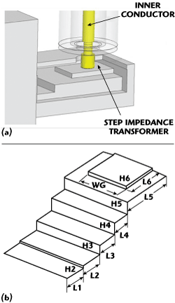
Figure 4 (a) transition assembly between the coasixal line and the step transformer and (b) step impedance structure.
The step impedance transformer structures have been studied and are used in this design. Figure 3 shows the overall structure used in the HFSS simulation. In the proposed design, the bottom of the coaxial inner conductor is in contact with the top of the step impedance transformer, as shown in Figure 4. The impedance of each section of the transformer is made equal to the geometrical average of the preceding and following segments. The length of each impedance step is approximately λ/4, equal to the electronic length θ =  . However, the length of this segment is not equivalent because the impedance depends on the propagation wave length in the waveguide
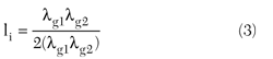
where λg1, λg2 are the lower and upper limits of the bandpass frequency, respectively. Naturally, there are n + 1 discontinuous points of impedance conversion for n rank impedance conversion. According to the dimensions of the 8 mm rectangular waveguide (3.556 × 7.112 mm), the length and height for each step impedance and of the actual device obtained by this method will be shorter by approximately 5/32 of a wavelength. Additionally, the fact that it is well matched with a wide range of frequency can be explained by the relatively constant characteristic impedance.
Simulation and Experimental Results
The whole waveguide-to-coaxial transition structure was simulated using the available HFSS. The outer conductor is made of copper (σ = 5.8 × 10⁷ Ω/m), while the inner conductor is made of MnCu alloy. The dielectric material is PTFE (er = 2.07), with a thickness of 1 mm.

Figure 5 Simulated field distribution, electric top, magnetic bottom; (a) non PBG structure and (b) PGB structure.
Figure 5 shows the electric and magnetic field distributions and Figure 6 the elec tric and magnetic line forces on the PGB structure in the inner conductor support within the coaxial line, as well as without PGB. The electric and magnetic fields are concentrated around the inner conductor, leading to improved transmission efficiency and less loss from the surface of the inner conductor support.

Figure 6 Electric (top) and magnetic (bottom) line of force: (a) non PBG structure and (b) PBG structure.
The structure was fabricated and tested. The vector network analyzer used for testing is Anritsu 37369B. Figure 7 shows the fabricated device and its simulated and measured VSWR. The simulation and measurement results agree quite well. The simulation shows that the VSWR is below 1.13 within the 26.2 to 40.6 GHz range with a VSWR of 1.102 at 37.5 GHz, while the measurements indicate that the VSWR is below 1.13 in the band of 24.2 to 37.9 GHz and is below 1.25 in the 37.9 to 40.6 GHz range. As mentioned before, such good performance is attributed to the use of the dielectric PBG structure that mitigates the transverse electromagnetic wave loss as well as improves the matching of impedances from waveguide to coax without additional parts.

Figure 7 Final test device (a) and VSWR curves (b).
Conclusion
In this article, an 8 mm coaxial to rectangular waveguide transition is proposed. It uses a dielectric PBG structure and a step impedance transformer and does not require additional parts such as tuning screws. Both simulation and measurement reveal that the designed adapter shows a VSWR result better than 1.2 within the frequency range of 26.2 to 40.6 GHz. Without additional screws, the whole structure is simple and stable, a perfect feature for use in the industry. n
References
- R.L. Eisenhart, P.T. Greiling, L.K. Roberts and R.S. Roretson, “A Useful Equivalence for a Coaxial-waveguide Junction,” IEEE Transactions on Microwave Theory and Techniques, Vol. 26, No. 3, March 1978, pp. 172-174.
- J.D. Joannopoulos, R.D. Meade and J.N. Winn, Photonic Crystals: Molding the Flow of Light, Princeton University Press, Princeton, NJ, 1995.
- A.G. Williamson, “Analysis and Modeling of ‘Two-Gap’ Coaxial Line Rectangular Waveguide Junctions,” IEEE Transactions on Microwave Theory and Techniques, Vol. 31, No. 3, March 1983, pp. 295-302.
- R. Beyer and F. Arndt, “Efficient MM/FE GSMS Technique for the CAD of Broadband Lateral Coax Feeds in Rectangular Waveguide,” 2000 IEEE MTT-S International Microwave Symposium Digest, pp. 109-112.
- A.G. Williamson, “Cross-coupled Coaxial-line/Rectangular-Waveguide Junction,” IEEE Transactions on Microwave Theory and Techniques, Vol. 33, No. 3, March 1985, pp. 277-280.
- K. Saitoh and M. Koshiba, “Photonic Bandgap Fibers with High Birefringence,” IEEE Photonics Technology Letters, Vol. 14, No. 9, September 2002, pp. 1291-1293.
- D. Labilloy, H. Benisty, C. Weisbuch, T.F. Krauss, R.M. De La Rue, V. Bardinal, R. Houdré, U. Oesterle, D. Cassagne and C. Jouanin, “Quantitative Measurement of Transmission, Reflection and Diffraction of Two-dimensional Photonic Band Gap Structures at Near-infrared Wavelengths,” The American Physical Society, Vol. 79, 1997, pp. 4147-4150.
- M.M. Radmanesh, Radio Frequency and Microwave Electronics Illustrated, Prentice Hall PTR, Upper Saddle River, NJ, 2001.