
The weakest signal that a wireless receiver can recover is defined by its sensitivity1
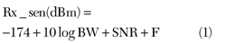
where BW is the bandwidth in Hz, SNR the required signal to noise ratio and F the system noise figure. A low-noise amplifier (LNA), as its name implies, improves the receiver sensitivity by reducing the cascade noise figure. Friis's equation shows that the noise figure (F1) of the first amplifying stage in the receiver chain (that is the LNA) has a predominant effect, while the noise performance of the subsequent stages (such as F2, F3, etc.) are of lesser importance. This is stated as

where Gn is the gain of the nth stage in the receive chain.
Cellular base stations (BTS) and microwave relays have detached low-noise amplifier stages located up in the aerial tower in order to mitigate the NF degradation from pre-LNA cable loss. In the BTS architecture, the LNA stage is preceded by a transmit-receive (Tx-Rx) diplexer for duplexing a common aerial and an interference filter for preventing out-of-band blocking or desensitization. However, both the duplexer and filter have losses that must be minimized as they occur before amplification.2 Therefore, an LNA with an extra margin in noise performance will relax the duplexer-filter's loss requirement.
Other critical performance parameters include high gain, to overcome loss in the long cable connecting the tower-mounted LNA and the ground-level radio shack, as well as high linearity, as the RF spectrum in the tower vicinity can be very crowded due to site sharing with other wireless transmitters.
A Brief Survey of Low-Noise Techniques
In the '70s and '80s, low-noise microwave amplifiers were mostly realized using ceramic-packaged devices3,4 because ceramic has extremely low loss (dissipation factor, tan δ = 0.001) and the stripline leads width could be matched to the PCB trace to minimize discontinuities. The shift to plastic surface-mount packaging (SMP) such as a SOT-23 or SC-70, for cost saving reasons, led to packaging that significantly degrades the noise performance because of the epoxy encapsulation's higher loss (tan δ = 0.006 to 0.0145) and also abrupt width changes at the die to bond-wire and led to microstrip interfaces.6
The Fukui equation for device noise7 can be simplified to demonstrate the proportionality of noise to physical temperature (TPHY)

Due to this relationship, lowering TPHY to near 0 K, using closed-cycle helium cooling, is by far the most effective noise-reduction method8 and has demonstrated F » 0.05 dB at 900 MHz.9 The improvement is attributed to better electron-transport properties and reduced thermal noise generated by parasitic elements.10 The flip side of cryogenic refrigeration is that it results in difficult maintenance11 and high cost (~$10k per cooler),12 thus limiting its use to performance-critical applications, such as radio telescopes and earth stations for interplanetary probes. Nevertheless, the future trend to replace a large radio telescope with thousands of smaller, low-cost ones distributed over a continent, such as the Square Kilometer Array,13 may make LNA cooling untenable.

In addition, the transistor's F is strongly influenced by the choice of semiconductor material. Cutting-edge materials, such as indium phosphide (InP), allow unrivalled noise performance, but are usually too costly for routine commercial use. On the other hand, silicon CMOS offers unbeatable cost benefits but has a modest noise level (see Table 1).
At the device level, shrinking the feature size (that is gate length) can improve most RF parameters.16 It has been shown that halving the CMOS feature size from 0.18 μm to 90 nm results in a useful 0.2 dB noise improvement at approximately 1 GHz,17 albeit at a significantly higher manufacturing cost.
Besides the device-level techniques, noise can also be reduced at the circuit level. The often significant difference between input conjugate match (ΓS) and optimum noise match (Γopt) of LNA transistors requires the noise performance to be sacrificed during matching. Nevin, et al. have shown that adding a small inductance (LS) in the source to ground path can minimize the ΓS - Γopt divergence;18 separately, a 0.15 dB noise reduction at 1.95 GHz has been reported using this technique.19 In practice, only a tiny less-than-ideal amount of LS can be added before undesirable peaks in the frequency response begin to form, far above the design pass band.20
FET-type devices have a relatively high optimum noise impedance (Zopt); connecting two or more transistors in parallel can lower noise by reducing the mismatch between Zopt and the generator impedance (Zs). Designs reported using this method include using three FETs in the 76 to 109 MHz VHF FM broadcast range21 and two HEMTs at 1.4 GHz.22
An input matching loss directly impacts F and the loss increases with the generator-to-input impedance transformation ratio (explained in the next section). The loss can be minimized by increasing the unloaded Q via a cavity23 or silver-plated resonators.24,25 However, these esoteric components are either too cumbersome or costly for mass-produced commercial products.
Feed-forward, a technique that is more commonly associated with power amplification, has also been described for noise reduction on CMOS LNAs26,27 at VHF/L-band. The noise produced in the input matching loss is combined in anti-phase with the output signal in order to cancel the noise components. However, a subsidiary noise amplifier and a combiner are required in addition to the LNA. This increased complexity may be the reason why feed-forward is still uncommon in commercial designs.

Figure 1 MMIC simplified circuit.
Device Physical and Parametric Characteristics
One approach is to use a compact (2 × 2 × 0.75 mm) 8-pin quad flat non-lead (QFN) packaged microwave monolithic integrated circuit (MMIC) that consists of a common-source amplifier and an active bias regulator. Its 0.25 μm feature-size GaAs enhancement-mode, pseudomorphic high electron mobility transistor (ePHEMT) process28 has a high gain-product bandwidth, fT >30 GHz, that allows the target gain (>17 dB at 0.9 GHz) to be achieved in one stage. The Johnson noise generated in the interconnections is minimized by making the metal two times thicker than in previous process iterations. A small source inductance (LS) enables good input return loss and F to be simultaneously achieved at one ΓS value (see Figure 1).
The gate width of the device was dimensioned to offer an input impedance close to 50 Ω in order to avoid requiring a large impedance transformation ratio in the external matching, which can increase losses and consequently degrade the noise figure F. The insertion loss (A) of a single transmission resonator at an evaluated frequency (f) is given by29

where f0 is the resonant frequency, Ql the loaded Q of the matching network and Qu the components' unloaded Q (usually the Qu of the inductor as it is lower than that of the capacitor). At the center of the resonator's pass band, f0 can be substituted for f; hence

The loaded QL of the matching network is given by30

where RH/RL is the resistance transformation ratio of the matching network. Substituting for QL gives

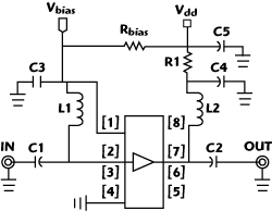
Figure 2 Performance evaluation circuit.
when RH/RL → 1, A ≈ 0 dB. That is, the lowest loss occurs when no impedance transformation is required. The best noise performance was extracted from this ePHEMT by dimensioning both the device geometry and its bias current to make the input close to 50 Ω, thus eliminating the input match requirement. The input inductor in the evaluation circuit (L1 in Figure 2) essentially functions as an RF choke only, and so its Q does not appreciably influence the input loss. The simulation confirmed the relative insensitivity to the resonator QUL (see Figure 3), where ΔF<0.05 for any QUL in the 20 to 100 range (the lower end of the range representing a 0402-size multilayer chip inductor and the upper end, a much larger air-core inductor). The uncritical input resonator requirement can enable low-cost and compact LNA designs.

Figure 3 Simulated 900 MHz noise figure vs. input resonator QUL.
The bias regulator allows the LNA quiescent current (Ids) to be adjusted by either varying RBIAS or an externally applied voltage, VBIAS (see Figure 4). The regulator's low current drive requirement (IBIAS ≤ 1mA) is compatible with most CMOS families, and it is possible to switch the LNA directly from a microcontroller in time domain multiplexed (TDM) applications. In applications that do not require this much linearity, an RBIAS value that is larger than nominal (6.8 kΩ) can be used to conserve power. The Ids temperature stability is achieved by the regulator and the LNA having undergone similar processing; that is, VBIAS and VGS "mirror" each other to compensate against thermal drift31 and between-wafer transconductance variation.

Figure 4 Characteristics of the adjustable bias regulator.
Performance Evaluation Circuit and Assembly
To evaluate the RF performance, a 900 MHz LNA for a cellular base station has been designed around the MMIC. A minimal number of external components (C1-L1 and C2-L2) provided the matching and biasing functions that were not feasible to integrate at the chip level. In addition to DC blocking and RF choking functions, C1-L1 also roll off undesirable gain below the operating frequency (f0). Both L1 and L2 should be operated below their self-resonant frequency (SRF) for effective choking. C3-C5 decouple the RF from the bias lines. In the interest of reducing the gain below f0, C4 is dimensioned for a reactance (X) of ~6 Ω at f0. Therefore, at f << f0, C4 gradually disappears from the circuit and R1 is directly in series with L1 to roll-off the gain. However, about 0.5 V is dropped across R1 at the nominal Idd of 50 mA and so the supply voltage Vdd must be raised to 5 V for Vds =4.5 V. When the LNA is switched via VBIAS as in TDM, C3 should be reduced to the lowest value that can still decouple the bias line effectively at f0; as a rule of thumb, XC3 = ~5 Ω at f0. The smaller C3 will speed up the switching that is constrained by the RBIAS - C3 time constant. Turn-on time is ~0.6 µs using C3 = 33 pF.
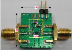
Figure 5 Photograph of the assembled prototype.
The printed circuit board (PCB) in Figure 5 measures 21.5 × 18 × 1.4 mm and comprises microstrips with co-planar ground on a 10 mil Rogers RO4350, a mid-priced material with modest RF performance and FR4-process compatible.32 A lower cost FR4 material of 1.2 mm thickness is glued to the RO4350 ground-plane for stiffening. RF connections were made through edge-launch SMA-to-microstrip transitions (Johnson Component P/N 142-0701-856), while the DC supply was connected via a two-pin straight PCB header. Because of the non-critical input resonator requirement, 0402-size chips could be used to shrink the area populated by components to approximately 8 × 10 mm. The evaluation board device list is shown in Table 2.

As preparation for the LNA circuit design, the MMIC was characterized with a custom-designed thru-reflect-line (TRL) fixture formed from the same PCB material (10 mil RO4350), which the prototype LNA was expected to use. After de-embedding the fixture effect, the device S-parameters and noise parameters were then imported into Agilent Technologies ADS2006A software for circuit simulation.

In the LNA circuit model illustrated in Figure 6, the RLC chip components were modeled using simplified equivalent circuits instead of the manufacturer-supplied s2p data; this was mainly because such data lacked the convenience of changing the component values instantaneously as needed. Secondly, such data were frequency limited to 6 GHz (so out-of-band stability could not be simulated). Additionally, the capacitor manufacturer's s2p data is severely limited in usefulness because its single reference plane lies along the chip's long axis33 and is therefore only accurate for a shunt-connected capacitor functioning as RF-to-ground bypass. A capacitor in series within the RF path, however, will require referencing to the metalized end terminals. To reduce the model complexity, only the most important parasitics ("first-order" parasitics) for the RLC components were modeled. The inductor model used typical QUL values at the nearest frequency (800 MHz) published by the vendor34 and extrapolated to other frequencies using a Q is proportional to √ƒ relation.
The inductors' parasitic capacitance (Cpst) was calculated from its published typical SRF values, but with an extra 0.1 pF added to account for layout capacitance. The parasitic inductance (Lpst) in the capacitor model followed the values provided by the vendor-supplied software, "Murata Chip S-parameter & Impedance Library."35
The two-pin header and its associated pads were excluded because they were found to have little impact on the simulated results. The edge-launched SMA jacks (female) were modeled using the ADS2006A parameterized component for coaxial line with the parameter values obtained from the manufacturer. However, discontinuity effects at the coax to micro-strip interface were ignored because the parameters are non-trivial to extract by either measurement or electromagnetic simulation.
Results and Discussion
The evaluation board nominal DC bias values are Vdd = 5 V and Idd = 53 mA (set by RBIAS = 6.8 kΩ). Key differentiators that will excite customers from the cellular BTS market segment are low noise in conjunction with good return loss (RL). This is because diplexers and filters are detuned by reflective terminations. At the 900 MHz nominal test frequency, the demonstration LNA achieved F ≈ 0.3 dB, G ≈ 18 dB and both IRL and ORL better than 15 dB.
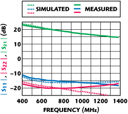
Figure 7 Simulated and measured S-parameters.
Traditionally, BTS LNAs rely on either isolator or quadrature hybrid coupler (balanced LNA) to achieve a desired input match. As shown in Figure 7, this design's low IRL allows the high-loss and costly isolator/quadrature coupler to be eliminated in most applications. The very wide bandwidth of the input and output match (0.35 to 6 GHz at the RL £ 10 dB point) is favorable from the system standpoint, as it prevents detuning of the input/output filters' out-of-band frequency response. Furthermore, there is reasonable agreement between simulated and measured G and RL at mid-band, where the differences are less than 2 dB.

Figure 8 Simulated and measured noise figure vs. frequency TPHY = 27°C.
As shown in Figure 8, the simulated F is ~0.15 dB higher than the measured result at f0. A discrepancy of this magnitude is not unusual and has been ascribed to a system-repeatability issue (an ATN source-pull system was used for device noise characterization, whereas a noise figure meter (Avago's 8970S) was used for the final measurement), as well as different samples or different day variations.36 Although the main target market is narrowband cellular BTS, the RF performances (F < 0.4 dB and RL < 10 dB in the 400 to 1400 MHz range) are also adequate for many wideband/multi-band applications such as cable/satellite TV distribution infrastructure, scanners, military applications and multi-service radios.

Figure 9 Measured and simulated wide-band gain and k factor.
As shown in Figure 9, the measured frequency response exhibited minor out-of-band "gain peaks" at 10, 13.5 and 18 GHz. But the peaks are well below the unity gain level, and so are not expected to create a potential instability if the LNA is inadvertently housed in a metal enclosure with a coincident cavity resonance. The Rollett stability factor (k) is greater than 1 when evaluated from HF to approximately >20 times the design center f0, meaning that the LNA will be unconditionally stable with any termination having a positive real part.
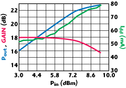
Figure 10 Output power, gain and Idd vs. input power.
Blocking, which desensitizes the receiver by lowering the G and increasing F,14 can be caused by either a non-synchronous interferer, such as a powerful transmitter sharing the same tower, or by a synchronous source, such as the transmission that leaks past the circulator or duplexer in a transceiver with simultaneous transmit and receive capability.38 A component with high gain compression threshold can therefore resist blockers more effectively. Gain compression is primarily caused by nonlinear transfer characteristics in an amplifier that is driven beyond the linear region with increasing heat dissipation as a minor contributor. In this design, heat loss is minimized by the GaAs substrate's comparatively lower bulk conductivity. Furthermore, the low knee voltage (0.3 V) of the selected process permits a larger voltage swing before clipping.39 The evaluation circuit's gain dropped 1 dB from nominal at an RF input drive (Pi) of 5.3 dBm. This corresponds to an output 1 dB compression point (P1dB) of 22.3 dBm. Due to the bias regulator's constant-voltage trait, the Idd rose exponentially with overdrive. The up-shifted bias point prevented premature waveform clipping as Pi approached P1dB. This similarity with Class AB mode improved P1dB over current-limited designs, as shown in Figure 10.
Due to receiver components' nonlinearity, adjacent-channel signals can create third-order intermodulation distortion (IMD3) such as 2f1-f2 or 2f2-f1 that virtually overlaps with the wanted signal. A key measure of linearity, the third-order intercept point, OIP3, is defined as the point where the fundamental signal power (Pfund) and the IMD3 power theoretically intersect. In the linear region, OIP3 can be calculated from the IMD3 amplitude using
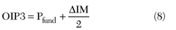

Figure 11 Fundamental, IM03 and OIP3 vs. Pi.
where ΔIM is the difference between the fundamental and the intermodulation product power in dB. Two input tones at 900 and 901 MHz were used for evaluating this design; however, a different frequency spacing is not expected to change the results much. In the linear operating region enclosed by Pi < -10 dBm, the OIP3 is slightly above 37 dBm at nominal bias, as shown in Figure 11. The key to high linearity at low power (as given by the linearity figure of merit, OIP3/PDC in Table 3; see page 66) is the processes' high transconductance (gm = 600 mS/mm) because harmonic distortion (such as 2f1) is inversely proportional to gm.15

The adjustable bias feature provides a convenient mean to trade-off OIP3 for power consumption (see Figure 12). The OIP3 can be varied as much as 10 dB by sweeping Idd over the 25 to 75 mA range while gain and P1dB are minimally affected (ΔG and ΔP1dB ≤ 0.5 dB). Microcontroller regulation of VBIAS opens the possibility to an LNA that can adaptively respond to a degree of spectrum crowding.

Figure 12 OIP3 vs. Ids.
Device Comparison
The optimization of several design parameters of a wideband low-noise, high-linearity LNA can enable critical performances equaling or exceeding that of traditionally used devices. As shown in the example used in this article, low-noise performance can be achieved by scaling the transistor size for almost zero input reflection coeffcient and minimizing internally generated thermal noise by using high-conductivity metallization. The resultant noise figure is comparable to that of ceramic devices. This design/device compares favorably with the prior art in key performance parameters, as shown in Table 3. Selecting a process with high gm can enable high linearity and best-in-class linearity figure of merit (OIP3/PDC). The relative insensitivity to input resonator Q can allow low-cost components to be used without sacrificing noise performance. The beneficial IRL over a wide bandwidth allows the isolator to be eliminated in most applications. Additionally, the low external component count makes possible a very compact LNA.
Acknowledgments
The author thanks M.D. Suhaiza and S. Punitha for assembling the prototypes, C.C. Loh for project leadership, S.A. Asrul for reviewing the paper, and the management of Avago Technologies for approving the publication of this work.
References
- Agilent Technologies Application Note, "AN57-1 Fundamentals of RF and Microwave Noise Figure Measurements," www.agilent.com.
- H.R. Ranson, A. Guyette and A. Abunjaileh, "Microwave Filter Design from a Systems Perspective," IEEE Microwave Magazine, Vol. 8, No. 5, October 2007, pp. 71-77.
- G.D. Vendelin, A.M. Pavio and U.L. Rohde, Microwave Circuit Design Using Linear and Nonlinear Techniques, John Wiley & Sons Inc., Somerset, NJ, 1989.
- O. Gorbachov, "Evaluation of Parasitic Parameters for Packaged Microwave Transistors," Applied Microwave and Wireless, Vol. 11, No. 4, April 1999, pp. 78-88.
- L. Li, A. Kapur and K.B. Heames, "Characterization of Transfer Molding Effects on RF Performance of Power Amplifier Module," 2004 Electronic Components and Technology Conference Proceedings," Vol. 2, pp. 1671-1677.
- K.R. Philpot, "A Guide to Microwave Diode Package Style and Their Performance," High Frequency Electronics, Vol. 4, No. 2, February 2005.
- D. Delagebeaudeuf and P. Briere, "MESFET Operation Principles and Device Modeling," The Microwave Engineering Handbook, Vol. 1, B.L. Smith and M.H. Carpentier, Eds., Chapman & Hall, London, UK, 1993.
- NRAO Webpage (2002), "Cooled HFET Amplifier Development," www.nrao.edu/engineering/amplifiers.shtml9.
- NRAO Webpage (June 2002), "Amplifier Performance as of May 1999," www.nrao.edu/engineering/ampperf-aug98.shtml.
- J.C. Webber and M.W. Popieszalski, "Microwave Instrumentation for Radio Astronomy," IEEE Transactions on Microwave Theory and Techniques, Vol. 56, No. 3, March 2002, pp. 975-985.
- M. Nisenoff and J.M. Pond, "Superconductors and Microwaves," IEEE Microwave Magazine, Vol. 10, No. 3, May 2009, pp. 84-95.
- G. Jones and S. Weinreb, "Thermoelectric Cooling of LNAs to 200 K," URSI 2005 Commission J Program for January 5-8, 2005 Boulder Meeting, http://astro.uchicago.edu/ursi-comm-J/ursi2005/.
- SKA Program Development Office (January 2010), "The Square Kilometer Array Fact Sheet," http://skatelescope.org.
- G.B. De Vaate, "RFIC Developments for Wideband Phased-array Systems," Perspectives on Radio Astronomy: Technology for Large Antenna Arrays, Dwingeloo, 1999.
- A.P. Chippendale, "Technology Issues for Square Kilometer Array Systems," Proceeding of the Workshop on Applications of Radio Science, Leura, February 2002.
- S.A. Maas, The RF and Microwave Circuit Design Cookbook, Artech House Inc., Norwood, MA, 1998, pp. 81-89.
- L. Belostotski and J.W. Haslet, "Noise Figure Optimization of Wideband Inductively-degenerated CMOS LNAs," International Midwest Symposium on Circuits and Systems, Montreal, Canada, August 2007.
- L. Neuvin and R. Wong, "L-band GaAs FET Amplifier," 1978 European Microwave Conference Proceedings, pp. 140-145.
- D.D. Henkes, "LNA Design Uses Series Feedback to Achieve Simultaneous Low Input VSWR and Low Noise," Applied Microwave and Wireless, October 1998, pp. 26-32.
- Avago Technologies Application Note, "AN1174: Low Noise Amplifiers for 1600 MHz and 1900 MHz Low Current Self-biased Applications Using the ATF-35143 Low Noise PHEMT," http://avagotech.com.
- K. Ishibayashi, "Amplifier for FM Antennas," United States Patent 6653905, November 25, 2003.
- N. Waldefalk, R. Gawande and S. Weinreb, "Very Low Noise Amplifiers at 300 K for 0.7 to 1.4 GHz," 2005 National Radio Science Meeting (URSI), http://astro.uchicago.edu/ursi-comm-J/ursi2005.
- J.J. Maintoux and F. Robles, "High Performance 432 MHz Preamp," Dubus Archives 8903-3, March 1989.
- C. Ward and D. Ward, "Preamplifiers," www.velalq.com/preamps/preamps.htm.
- C. Bartram, "1.3 GHz HEMT Tropo Preamp," www.christopherbartramrfdesign.com/blaenffos/projects/1preamp.htmlg3.
- F. Bruccoleri, "Wideband CMOS Low-noise Amplifier Exploiting Thermal Noise Cancelling," IEEE Journal of Solid State Circuits, Vol. 39, No. 2, February 2004, pp. 275-282.
- S.A. Jackson, "RF Design of a Wideband CMOS Integrated Receiver for Phased-array Applications," Experimental Astronomy, Vol. 17, No. 1-3, June 2004, pp. 201-210.
- K. Fujii and H. Morkner, "Single Supply 1 W Ku-band Power Amplifier Based on 0.25 gm E-mode PHEMT," 2006 IEEE MTT-S International Microwave Symposium Digest, pp. 1855-1858.
- K.V. Puglia, "A General Design Procedure for Bandpass Filters Derived from Low Pass Prototype Elements, Part I," Microwave Journal, Vol. 43, No. 12, December 2000, pp. 22-38.
- C. Bovick, RF Circuit Design, Howard W. Sam, Carmel, IN, 1982, p. 68.
- C. Blair, "Biasing LDMOS FET for Linear Operation," Applied Microwave & Wireless, January 2000, p. 92.
- Rogers Corp. Product Specification, "RO4000 Series High Frequency Circuit Materials," rev. 1. www.rogers-corp.com.
- Murata Inc. Product Specification, "About Characteristic Parameters of Murata Component Library," http://murata.com.
- Toko Inc. Product Specification, "LL1005FHL Multilayer Chip Inductor," http://www.tokoam.com.
- Murata Manufacturing Software, "Murata Chip S-parameter and Impedance Library, Version 3.6.0," 2004.
- C.A. Morales-Silva, L. Dunleavy and R Connick, "Noise Parameter Measurement Verification by Means of Benchmark Transistors," High Frequency Electronics, February 2009, pp. 18-25.
- W. Domino, N. Vakilian and D. Agahi, "Polynomial Model of Blocker Effects on LNA/Mixer Devices," Applied Microwave & Wireless, June 2001.
- O.K. Jensen, et al.,"RF Receiver Requirements for 3G W-CDMA Mobile Equipment," Microwave Journal, Vol. 43, No. 2, February 2000, pp. 22-46.
- D.W. Wu, et al., "An Enhanced-mode PHEMT for Single-supply Power Amplifiers," HP Journal, February 1998.
- California Eastern Laboratories Application Note, "AN82901-1 Application Microwave GaAs FET," www.cel.com.
- D.R. Huanh, H.R. Chuang, Y.K. Chu and C.L. Lu, "A 40 to 900 MHz CMOS Broadband Differential LNA for a DTV RF Tuner," Microwave Journal, Vol. 50, No. 2, February 2007, pp. 128-136.
- L. Belostotski and J.W. Haslett, "Noise Figure Optimization of Wideband Inductively-degenerated CMOS LNAs," 2007 IEEE International Midwest Symposium on Circuits and Systems Proceedings, pp. 1002-1005.
- C. Enguenhard, V. Armengaud, J. Lintignat, B. Barelaud, B. Jarry and L.I. Babak, "Low-noise Amplifier Design with Metamorphic HEMT Technology for Radio Astronomy Application," Proceedings of the Wide Field Science and Technology for the Square Kilometer Array, Belgium, 2009.
- RFMD product Specification, "SPF-5189Z," www.rfmd.com.
- RFMD Product Specification, "RF3863," www.rfmd.com.
- Hittite Product specification, "HMC617LP3," www.hittite.com.