
The design of a highly integrated Ka-band TX front-end module is presented. The integration and packaging techniques, which combine the LTCC front-end module with the LO signal generation board, the IF distribution board and the cooling system are considered in detail. The efficient RF design process of the different functional blocks of the LTCC module (antenna elements including hybrid ring feeds, calibration network, 30.6 GHz LO distribution network, active RF circuits, liquid cooling and DC supply), includes full wave EM simulations. During design, it is necessary to carry out EM simulation of the complete front-end module to check for parasitics and layout errors. The manufacture of the demonstrators in LTCC technology is explained and measurement results are presented. The front-end achieves a scan range of ± 60°, EIRP is approximately 40 dBm and the operating frequency band is 29.5 to 30 GHz. This modular system concept can be applied to large antenna arrays in order to fulfill link budget requirements for satellite communication (in this instance) as well as for other phased-array applications.
Future satellite systems, operating at Ka-band frequencies, will provide high data rates, enabling applications such as in flight entertainment in airliners. In the near future, aircrafts could be equipped with electronically steerable antennas, such as those based on digital beam forming (DBF). Electronically steerable antennas based on DBF offer greater flexibility in beam control and are more mechanically robust than mechanical systems. However, the hardware development effort is greater, due to the increased complexity of the system.
At higher frequencies (such as Ka-band, as considered here), the packaging density is very high, which requires suitable system architectures and technologies to handle such a complex level of integration. The combination of the active RF circuit with the antenna in one module decreases the number of high frequency interconnects and reduces the total size significantly.

Figure 1 3D model of the 64 × 64 element array and the single assembled TX front-end.
TX Front-End Overview
The TX front-end is designed with a modular approach. Each front-end consists of a LTCC module with an 8 × 8 patch antenna array and integrated RF electronics, a LO board, IF boards and cooling elements (see Figure 1, right side). Several modules can be combined to form a larger array to fulfill the budget requirements necessary for the specific application. A larger antenna where 16 modules have been combined to form a 64 × 64 element patch antenna array is shown on the left side of Figure 1.
This modular approach results in a design where all RF and DC electronics, including cooling, must fit behind the antenna. The antenna for each patch element is limited by the antenna element spacing, which is half a wavelength. A larger distance between the antenna elements would degrade the antenna performance with respect to the sidelobe level, grating lobe level and scan range. The antenna element area for this Ka-band antenna design is 5 × 5 mm.
This is a small space, especially for a DBF antenna, as each patch element needs its own chipset consisting of mixer, filter, PA with IF and DC connections to allow for amplitude and phase control at the baseband level. The solution proposed here is a vertical integration of the different functional blocks. Most RF parts have been integrated in a multilayer LTCC module. LTCC technology was chosen due to its flexibility for a multilayer circuit design with a high integration density.
The main parts of the complete TX front-end are the highly integrated LTCC module, the IF distribution boards with DC supply, a board for the 30.6 GHz LO signal creation and the cooling elements. The LO signal is routed with mini SMP connectors from the RF LO board to the LTCC module. An 80 pin connector is used for routing the 64 IF signals, together with several ground connections to the main IF distribution board. Two flex cables connect the IF signals to the second and third IF distribution board from which the IF signals are routed to a rack with the baseband DBF channel boards.

Figure 2 3D view from the RF circuit side of the LTCC front-end module.
The DC signals are routed with four DC connectors via the IF distribution boards to the DC input connectors. The cooling channels of the LTCC module are connected to an external cooling system by pipes, together with the LO heatsink.
LTCC Module Design
The multilayer LTCC module consists of 17 tapes with 18 metallization layers. The following system functionalities of the front-end are integrated: antenna array, including calibration network and hybrid ring feed, RF circuits and cooling system. Figure 2 shows the RF circuit side of the front-end module obtained from the EMPIRE XCcel EM simulation model.

Figure 3 3D view of the main functional layers from the LTCC module.
The antenna front-end consists of 8 × 8 antenna elements, with separate hybrid ring feed for each element, and an integrated calibration network.1-3 One edge of the module with the main functional layers is shown in Figure 3. The antenna elements are red and the hybrid ring feed, which is located above the antenna, is purple. Two via holes connect the 0° and 90° output of the hybrid ring feed with the patch antenna (not shown in the figure). The calibration network (green) collects a small amount of the antenna signal with two probes at each patch.
Wilkinson dividers are used to combine the calibration signal of 16 patches at the calibration receivers (four in total). An interconnection layer (black) in the middle of the LTCC connects the signals of the antenna feed to the output of the PA. This routing layer is necessary as the chipsets of the different antenna patches cannot always be placed directly above the antenna due to the placement of the different connectors (IF connector, LO connectors, DC connectors) on the RF circuit side.
The LO distribution network (yellow) consists of two 1:32 dividers to feed the RF transmitting chip sets, with two additional output ports for the down converters (signal calibration). The DC networks (grey) for gate and drain voltage that supply the PAs are placed between the LO and IF network. One DC network is used to feed 16 PAs. A symmetrical DC routing for each quarter of the module is necessary to ensure a stable operation of the PAs. The two IF networks (brown) connect all 64 mixers to the central IF connector.
The inlet of the cooling system (yellow) and the cooling channels (blue) are shown in Figure 2. Beneath the RF chipsets, inner cavities in the LTCC are used to form a pipework for the cooling system. The RF transmitting chip sets (grey) comprise one amplifier, filter and one mixer (up-conversion) per antenna element. These are located on the RF circuit side of the LTCC module, as shown in Figure 2. Four additional mixers (down conversion) are needed for calibration purposes.
All the different parts of the LTCC TX front-end have been designed and analyzed using the EMPIRE XCcel 3D-FDTD field solver. The design flow for this LTCC module started with the design of the patch antenna, the 90° hybrid circuit and the calibration network. Next, the RF chipsets were integrated, together with the connectors on the surface of the LTCC. The LO network and the IF network were designed later. Finally, the antenna and the RF parts were integrated into one LTCC module. It is important to simulate the complete module with a full wave EM simulation tool.
The simulation of the antenna path starts with a microstrip port at the power amplifier. An impedance transformer and a matching circuit at the top of the LTCC matches the integrated 30 Ω 90° hybrid circuit to the 50 Ω output of the power amplifier. The simulation of the 30.6 GHz LO signal starts at the two mini SMP connectors with a coaxial port and ends at the 64 mixers and at the calibration receivers with microstrip ports. This simulation technique includes all parasitic couplings between the different elements. A retuning of the LO network and some antenna paths had to be applied to compensate for these parasitics.
In addition to the RF characterization, the complete module simulation facilitates the checking of layout errors such as shorts or open circuits. This simulation technique ensures a short turnover from design to manufacturing even for such a complex design, with more than 40,000 objects. The simulation of the complete LTCC module needs just approximately 16 GB memory and a simulation time below four hours on a PC cluster of seven standard Intel Core i7 920 PCs. A single dual Xeon 5580 workstation needs about nine hours for the simulation.
LTCC Module Manufacturing and Assembly
The complete LTCC module was realized through 17 tapes of Ferro A6M, which was chosen due to its low loss (tan δ = 0.002) and low permittivity (εr = 5.8), compared to other LTCC materials.
The first tape at the RF circuit side has a fired thickness of 96 μm to enable a higher integration density, while using 50 Ω microstrip lines on the surface. All other tapes have a thickness of 190 μm. Gold paste was used for all internal metallization, vias and at the outer layers, where no soldering of connectors is necessary. A solderable paste (Pt, Pd, Au) was used in the area where the DC, LO and IF connector as well as the cooling inlet and outlet have to be soldered. No post firing process was applied.

Figure 4 Photograph of the LTCC module, including mounted connectors and chipsets.
General design rules are a fired minimal line width of 100 μm and a minimal line spacing of 100 μm. The fired via diameter is 170 μm. Cavities are used on both sides as well as inside the LTCC. A sacrificial material was used for the inner cavities for the lamination and burn out process to guarantee a good shape of the inner cavities (cooling channels).
A photograph of the RF circuit side from the first prototype of the LTCC module is shown in Figure 4. The x-y direction shrinkage of the LTCC module during the firing process was very stable and varied only between 15.9 and 16.2 percent for 10 different tiles.

Figure 5 Cross cut through the cooling channels of the LTCC module.
To analyze manufacturing accuracies, including for the inner layers, one tile was cut into several slices. A cross-section through a cooling channel, located directly beneath the RF chipsets, is shown in Figure 5. It is clear that the thermal via holes, which are located directly beneath the amplifiers, allow for good thermal conduction between the amplifiers and cooling channel. The cooling channel is two layers high (380 μm), except in the area where transversal tape connections were necessary during production.
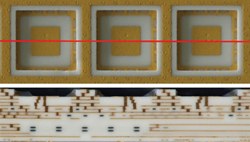
Figure 6 Cross cut through antenna feed and cavity.
The input to the cooling channel is at the right side at the junction to the main channel. A cross-section of the antenna elements is shown in Figure 6. The antenna cavities, shielded by via fences, can clearly be recognized, as well as the antenna via feeds and shorting vias in the middle of the antenna patch elements. The shorting via in the center of the patch enhances the polarization purity and the placement of the patches in the cavities reduces the coupling in between the patches. There is a good alignment between the different tapes (better than 50 μm).
The manufacturing of inner and outer cavities in LTCC is difficult as the high lamination pressure (3,000 psi) often causes deformation. To overcome this problem a sacrificial material is placed inside the cavities. This material is completely removed automatically along with the organic contents of the LTCC tape in the burn-out-phase (350°C … 600°C), leaving accurately shaped cavities behind.

Figure 7 Simulated and measured return loss at the microstrip interface.
After the manufacture of the LTCC tile and initial test measurements were taken, the IF, DC and LO connectors were soldered, and all the 64 transmitting channels of the module were equipped with the RF chipsets. The RF chipsets consist of a mixer (Hittite HMC 329), an IF filter (specific design) and a PA (Avago AMMC 6232, output P1dB = 20 dBm, small-signal gain = 27 dB, 18 to 32 GHz). These chipset components were mounted to the LTCC with conductive glue.
Measurements
The interface between the PA output and the LTCC was designed in a way that on wafer probe measurements can be done to check the functionality of all 64 antenna elements on the LTCC, before the PA is glued and bonded. For these test measurements, each element is contacted on the microstrip RF interface. A sheet absorber material was used on the antenna side to absorb the radiated fields and prevent a reflection at the metal chuck. Figure 7 shows the measurement and simulation results of the return loss at this microstrip RF interface.
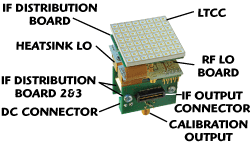
Figure 8 Assembled TX front-end module.
One element was singled out and the variation on one module and between different modules was investigated. Each antenna element exists twice on one LTCC module as the upper part can be created by rotating the lower part by 180° around the centre of the whole module. It was found that the return loss of the elements is better than 10 dB over the complete operating frequency band (29.5 to 30 GHz). The agreement between the different curves is excellent and shows good production accuracy. The small discrepancies to the simulation results can be explained because of the deviations in the material parameters and in LTCC shrinkage tolerances. The prototype of the assembled TX front-end module is shown in Figure 8. This front-end module contains the complete assembled and tested LTCC module, the RF- and LO-boards and the cooling system.
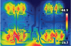
Figure 9 Surface temperature of the LTCC module with active PRS.
The cooling system of the LTCC module was tested before calibration. DC gate and drain voltage were applied to all PAs after activating the cooling system. Excellent temperature behavior was observed by surface temperature measurement with an infrared camera (see Figure 9). The surface temperature on the PA chips and in the surrounding area stayed below 50°C. Thermal via holes connecting the bottom of the PA chips directly with the cooling channel reduce the PA temperature even more than the temperature in the surrounding area. The large margin between the currently measured PA temperature (< 50°C) and the maximum operating temperature of the PA (~ 150°C) could facilitate a change from a liquid cooling fluid to air.
The far-field behavior of the steered 8 × 8 antenna array was determined using an active measurement setup. The antenna was connected with the baseband system to a PC with graphical user interface for amplitude and phase control at the baseband level. All elements can be digitally controlled (DBF) in amplitude and phase. Thus, the 8 × 8 antenna array can be set to different scanning directions, of which the far-field patterns can then be recorded.

Figure 10 Measured co-polar far-field pattern.
Figure 10 shows the measurement results for the right-hand circular-polarization (RHCP), that is the co-polar component for different scanning angles without any amplitude tapering. The scanning behavior is very good and symmetric in each direction. The maximum scanning loss appears at ±60° and is only approximately 3.5 dB. The side lobe level is below -8 dB for all scanning angles, which corresponds well with the theoretical values for uniform amplitude assignment.
Conclusion
A highly integrated TX front-end module design, with an integrated 8 × 8 array antenna module, has been presented. The combination of the RF circuit on the one side of the LTCC module and the antenna on the other side saves space and reduces the number of high frequency interconnects compared to a solution with separate modules for all RF circuits and the antenna.
Due to the compact layout of the antenna and the corresponding RF circuitry on the back of the antenna, it is possible to use the 8 × 8 antenna as a base block for larger antenna arrays. The measurement results show a very high reproducibility in the LTCC manufacturing process. The digital control for all elements in amplitude and phase enables scanning angles up to ± 60°.
Acknowledgments
The authors wish to acknowledge the funding of this work within the framework of the SANTANA 3 project by the German Aerospace Center (DLR) on behalf of the German Federal Ministry of Economics and Technology (BMWi) under research contract 50YB0710. The background and vision of this project are given in Reference 4.
References
- O. Litschke, W. Simon and S. Holzwarth, “A 30 GHz Highly Integrated LTCC Antenna Element for Digital Beam Forming Arrays,” 2005 IEEE Antennas and Propagation Society International Symposium Digest, Vol. 3B, pp. 297-300.
- S. Holzwarth and O. Litschke, “8 × 8 Element Digital Beam Forming Antenna Array for Ka-band,” 2006 Proceedings of the European Conference on Antennas and Propagation (EuCAP).
- S. Holzwarth, O. Litschke, W. Simon, K. Kuhlmann and A.F. Jacob, “Far-field Pattern Analysis and Measurement of a Digital Beam Forming 8 × 8 Antenna Array Transmitting from 29.5 to 30 GHz,” 2007 Proceedings of the European Conference on Antennas and Propagation (EuCAP), pp. 1-5.
- S. Holzwarth, A.F. Jacob, A. Dreher, C. Hunscher, D. Zahn, F. Woetzel, H. Fischer, A. Geise, R. Gieron, K. Kuhlmann, O. Litschke, D. Lohmann, W. Simon and A. Stark, “SANTANA: Advanced Electronically Steerable Antennas at Ka-band, Project Status and Outlook,” 2010 Proceedings of the Fourth European Conference on Antennas and Propagation (EuCAP), pp. 1-5.
Winfried Simon joined IMST GmbH in Kamp-Lintfort, Germany, in 1996, and is currently working as a senior engineer in the department of Antennas & EM Modelling.
Jürgen Kassner works in the RF Modules subdivision of the RF Circuits and Systems department of IMST GmbH.
Oliver Litschke works with IMST GmbH, Kamp-Lintfort, Germany, in the Antennas & EM-Modelling department.
Horst Fischer joined IMST GmbH, Kamp-Lintfort, Germany, in 1999, working in the RF Circuits and System Integration department.
Sybille Holzwarth works in the Antennas & EM-Modelling department of IMST GmbH, Kamp-Lintfort, Germany.