
Measuring electromagnetic properties of materials can provide insight into applications in many areas of science and technology. Increasingly, these properties need to be evaluated at the nanometer scale. Since electromagnetic properties, such as the dielectric constant, are ultimately related to a material’s molecular structure, correlating the detailed physical structure of a material with its electromagnetic properties is frequently more valuable than the knowledge of either alone.
Developed by Agilent Technologies, scanning microwave microscopy (SMM) is a technique that combines the compound, calibrated electrical measurement capabilities of a microwave vector network analyzer (VNA) with the nanoscale spatial resolution and angstrom-scale positioning of an atomic force microscope (AFM) (see Figure 1). This unique method allows the measurement of highly localized capacitance, dopant density, charge distribution and dielectric properties on a broad variety of samples, thus offering the semiconductor industry a host of new application possibilities.

Figure 1 Scanning microwave microscopy system.
SMM outperforms traditional AFM-based scanning capacitance microscopy techniques by providing higher sensitivity and dynamic range, the ability to acquire quantitative results, and greater application versatility. SMM works on all classes of semiconductors: Si, Ge, III-V (such as GaAs, InAs, GaN) and II-VI (such as CdTe, ZnSe). Unlike traditional scanning capacitance microscopy, it does not require an oxide layer.
SMM can also be used on dielectric materials, ferroelectric materials, insulators and biological materials to measure properties associated with small variations in the electromagnetic interactions of a sample’s different components with the incident microwave signal, either statically or dynamically. Data from representative samples demonstrate that SMM is capable of mapping material properties at a resolution ultimately limited by the sharpness of the AFM probe.
The Role of the VNA
The vector network analyzer utilized to perform SMM is a state-of-the-art characterization instrument that makes extremely accurate, calibrated measurements of complex-valued ratios on electromagnetic signals. The ratios are R = reflected signal/incident signal and T = transmitted signal/incident signal.
The incident signal is generated and controlled inside the VNA; as a result, the ratios R and T are not merely relative, but referenced to the well-known, accurately quantified incident signal. This measurement capability, delivered to the apex of an AFM tip, enables calibrated, traceable measurements of electrical properties such as impedance and capacitance.
The VNA is a stimulus-response instrument, optimized for accurate and repeatable measurement of the response of a network or a device under test (DUT) to a known stimulus signal. This is in contradistinction to instruments, such as the spectrum analyzer, which are usually configured simply as a receiver of an unknown signal and which do not include a source for a stimulus to be applied to the DUT.
The VNA has two operational modes: transmission and reflection. In the reflection (alternatively, transmission) mode, the VNA measures the magnitude and phase characteristics of the DUT by comparing the signal that reflects off (alternatively, transmits through) the device with the stimulus signal. Each of the two modes enables measurement of several useful parameters. For instance, in the reflection mode, the VNA can measure the impedance of the DUT (such as the total resistance that a DUT presents to the flow of an AC signal at a given frequency).
Scanning Impedance Microscopy
One of the most common applications of network analysis is measuring the impedance of a component, so as to evaluate if it matches the impedance of the other components with which it must interface in a network. In SMM, the reflection mode of the VNA is used for measuring the impedance of a “network” that includes the tip-sample interface. Here, the DUT for the VNA consists of the AFM probe and the region of the sample immediately beneath the metal AFM tip. The incident microwave signal travels through a series of components before it reaches the tip-sample interface by means of a transmission line. The impedance mismatch between the transmission line and the DUT causes the incident microwave signal to partially reflect from the tip-sample interface back towards the stimulus signal source inside the VNA; this reflected signal is proportional to the impedance mismatch. The incident microwave signal and the reflected microwave signal together contain information about the impedance of the DUT.
Impedance can actually be measured in three different ways with a VNA, according to the frequency and the magnitudes involved. The reflection method of measuring impedance is the one that works best at microwave frequencies and for impedance values at or near the characteristic impedance of transmission lines (50 or 75 Ω). The accuracy of a VNA impedance measurement diminishes, however, as the impedance values move away from these characteristic values.
SMM’s VNA-based impedance measurement technique is a simple yet effective scheme that brings the instrument’s reflection-mode measurement capabilities to bear upon solving the problem of measuring with a very high resolution the small changes of a very small impedance (capacitance), that is that of the MOS capacitor (AFM tip/semiconductor) to the RF ground.
The magnitude of the complex-valued reflection coefficient S11 changes with both the load impedance ZL and the source impedance ZS (internal to the VNA) as follows:

The complex-valued reflection coefficient S11 is one of four scattering parameters (S-parameters) that are used to characterize the response of a DUT at high frequencies in a way consistent with transmission line theory. All four S-parameters are ratios of voltage traveling waves entering and exiting the DUT. When the value of ZL is close to that of ZS, the plot has the steepest slope, which corresponds to the highest sensitivity and the highest resolution. ZS is 50 Ω, but ZL is generally not near this value.
In order to bring the value of ZL closer to that of ZS and therefore exploit the VNA’s impedance measurement capability in its most accurate and sensitive range, SMM uses a half-wavelength impedance transformer to place the measurand, the DUT, directly across an external 50 Ω impedance (that is parallel to it). In this way, SMM operates the VNA with the sensitivity and resolution required to measure capacitance changes on the order of 0.1 aF across a 0.1 fF base capacitance. Furthermore, this impedance transformation is done at a location that is physically remote from the tip-sample interface, thereby facilitating mechanical design implementation.
The results for this setup show that the VNA now operates with a resonant structure as its load, thus enabling it to measure minute changes in the value of the capacitance-to-ground in the highest sensitivity range of the VNA.
Scanning Capacitance Microscopy
One application of impedance measurement with SMM is scanning capacitance microscopy (SCM) of semiconductors. Measuring the capacitance-to-ground (C) of the tip-sample interface and its variation (dC/dV) with an applied AC bias (V = V0 sin ωt) is an important extension of atomic force microscopy for the electrical characterization of semiconductors. It enables two-dimensional mapping of the carrier density across different regions of a semiconductor, with applications in the failure analysis, characterization, modeling and simulation of device performance, as well as in the development of the semiconductor fabrication process.
Traditionally, a resonant capacitive sensor-based SCM technique has been used to implement this type of AFM technique with some success. One of the main shortcomings of traditional SCM is the difficulty of making absolute measurements of the strength of the tip-sample electrical interaction; therefore, SCM images remain maps of the relative difference in carrier densities across the scanned area. For this reason, accomplishing the much coveted task of using SCM to reliably and repeatably extract numerical estimates for carrier densities in semiconductor devices remains elusive.
The VNA hardware utilized in SMM includes precision components for the calibration and performance verification of the instrument, thereby extending its applications to those that require calibrated, traceable and absolute measurements of capacitance, for example.
Capacitance Calibration Process
In order to achieve quantitative capacitance measurements, calibration samples were fabricated on a single-side polished Si wafer using customary deposition, etching and photolithographic procedures. These samples consist of a series of micro-capacitors that vary in lateral dimension and dielectric thickness. The calibration capacitance sample was developed as a parallel plate capacitor, with the SiO2 dielectric sandwiched in between the plates. The two plates correspond to the gold caps (in electrical contact with the conductive AFM-tip), and the circular regions of silicon below the dielectric material.
For routine capacitance calibration, gold pads of 3 μm diameter were used. However, a second capacitance proportional only to the cap area, but not dependent on the thickness of the dielectric layer, had to be considered (abbreviated as Cback on the equation below). The two capacitors, Cdiel and Cback are in series. The two capacitors in series result in the following model for the total measured capacitance Ctot:

with Cdiel being the capacitance of the SiO2 capacitor, Cback the background capacitance, A the pad area, d the dielectric step height and e the dielectric constant.

Figure 2 Reflection amplitude data on the 50 nm stepped sample acquired by VNA at 2 GHz.
Scanning microwave microscopy’s calibrated measurements and high-resolution imaging of capacitance-to-ground between an AFM tip and a semiconductor sample enables reliable, repeatable, extraction of numerical values of the carrier densities in a semiconductor. SMM typically operates at microwave frequencies of 2 to 16 GHz, which is substantially higher than the frequencies used in traditional SCM (approximately 900 MHz). The higher frequencies in SMM lead to better sensitivity and electrical resolution for measuring the tip-sample capacitance. SMM uses a lock-in amplifier for measuring the in-quadrature and in-phase components of dC/dV, allowing the determination of the polarity of the majority carriers in the semiconductor (see Figure 2). Figure 2a shows the VNA amplitude image with a scan size of 60 × 60 μm. Figure 2b shows that a topographical image at the same scan size was simultaneously attained. For each gold pad, the |ΔS11| amplitude value was determined and plotted versus the gold pad area, as shown in Figure 2c. The data is shown for the four different steps of the dielectric staircase structure. A plot of the inverse amplitude |ΔS11| with respect to the dielectric step height ranging from ≈ 50 nm to ≈ 200 nm is shown in Figure 2d.
The Role of the AFM
To take full advantage of the VNA-based measurement scheme, SMM incorporates several innovations into the AFM hardware. These include a sophisticated microwave shielding to improve the instrument’s electromagnetic compatibility with its surroundings and minimize the effect of stray capacitances, which are inevitable with the probe’s movement during raster scanning. The innovation of this design is implemented in such a way as to minimize the impact on the performance of the AFM scanner, where the cantilever holder attaches to the rest of the AFM.
In SMM, the VNA sends an incident microwave signal through a diplexer microcircuit to a sub-7 nm conductive tip of a platinum-iridium cantilever. The AFM scans the tip over the sample and can move the tip to specific locations to perform point probing. SMM utilizes a multipurpose AFM scanner, either open- or closed-loop, capable of scanning areas up to 90 × 90 µm. When equipped with a 200 × 200 mm stage, samples up to 8" in diameter and 30 mm tall are easily accepted.
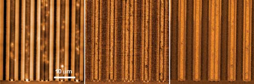
Figure 3 SMM images of a doped SiGe device.
Custom software controls the data acquisition of all channels for SMM, including topography from the AFM controller, amplitude and phase of the reflection coefficient from the VNA, and the dC/dV components from the AC mode controller. The software saves all SMM data in 32 bit format to preserve the dynamic range of the data. Figure 3 shows images of a doped SiGe device, acquired with scanning microwave microscopy. On the left is the topography, in the middle the capacitance, and on the right dC/dV.
Semiconductors and Beyond
Scanning microwave microscopy is particularly useful for semiconductor test and characterization. Applications include highly localized measurements of impedance, capacitance and dielectric properties. The technique paves the way for extracting reliable numerical estimates of the carrier densities in semiconductors from the impedance (capacitance) data.

Figure 4 AFM topography and dC/dV images of SRAM.
Exceptionally high electrical and spatial resolution also make SMM well suited to a wide range of biological and materials science applications, including the characterization of interfacial properties. As well as its ability to work on semiconductors, glasses, polymers, ceramics and metals, the technique lets researchers perform high-sensitivity investigations of ferroelectric, dielectric and PZT materials. Studies of organic films, membranes and biological samples can also benefit from the use of SMM. Its very high sensitivity (1.2 aF) is suited for looking at ion channels in cell membranes. It is anticipated that SMM-enabled nanoscale measurement capabilities will be expanded to include sweep frequency and spectroscopy volume in the near future. Figure 4 shows the AFM topography (A and C) and dC/dV (B and D) images of SRAM.
C and D are zoom scans of one of the transistors in the n well marked in the blue square in A/B. A very fine line feature of 10 to 20 nm in width can be seen in the dC/dV image, as pointed in D, indicating high resolution capability of the scanning microwave microscope.