
Ultra-wideband (UWB) is a technology for transmitting information spread over a large bandwidth that should be able to share spectrum with other users. This is the main reason why UWB has attracted much attention from the wireless community, both from standardization bodies and chip manufacturers. The UWB frequency range is from 3.1 to 10.6 GHz and the data rate is up to 480 Mbps.1,2
One of the most challenging components of a UWB front-end is the wideband low noise amplifier (LNA). This circuit must have a precise amplification over a wide range of frequencies. There are several methods to design a UWB LNA. Previously reported articles use the classic shunt-feedback configuration.3-5 Another commonly used topology is the distributed amplifier,6-8 where several gain stages are connected so that their capacitances are separated. Series inductive elements are used to separate capacitances at the inputs and outputs of adjacent gain stages occupying a high area. Finally, inductor degenerated amplifiers with LC-ladder input matching networks are also employed.9-11 This configuration expands the use of the typical inductively degenerated narrow band amplifier, by embedding the input network of the amplifying device in a multi-section reactive network. In this way, the overall input reactance is resonated over a wider bandwidth, achieving at the same time a wideband input match and low NF. To extend the gain bandwidth, the load is generally composed of a shunt-peaking resistor.12 This technique imposes an upper limit to maximum gain and flatness. To overcome this issue, a modification of the conventional shunt-peaking load is proposed.

Figure 1 Wideband LNA simplified schematic with wideband input impedance matching.
Circuit Description
A schematic of the wideband input matched CMOS LNA is shown in Figure 1. It consists of a wideband input matching circuit, a gain stage with inductive degeneration (Lg and LS)11 and a wideband output load. In order to buffer the output to an external 50 Ω load, an emitter follower (M3) has been included. As the figure shows, the input matching circuit consists of a filter embedded with the input impedance of M1. In this case, a third-order bandpass Chebyshev filter in T configuration was selected. In order to increase the flexibility of the filter, CP is introduced between the gate and source of M1.
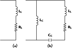
Figure 2 Conventional shunt-peaking load (a) and modified shunt-peaking load (b).
The gain stage is composed of a cascode transistor, which improves the reverse isolation and lowers the Miller multiplied capacitance. The width and polarization current of the transistors are optimized for noise and power consumption. As shown in Figure 2, and in order to provide a wideband operation, the typical resonant load used in narrow band LNAs is replaced by a shunt-peaking resistor.12 With this configuration the overall amplifier gain should be flat across the pass-band. The amplifier gain is given by the product of the transistor transconductance (gm) and the magnitude of the impedance of the shunt-peaking load, given by:
where Cout represents the equivalent capacitance at the output node, which includes the transistor output capacitance, the loading by interconnections and subsequent stages, and the parasitic capacitance of the inductor. This expression contains a zero and two complex poles. The extended bandwidth comes from the |Z(jω)| increase due to the poles below the LLCout resonance (ω0 = 1/LLCout) and to the zero (ωz = RL/LL). Unfortunately, this leads to a peak in the frequency response, thus degrading the flatness. A possible solution is to keep both resonances out-of-band by using a low value of LL, which in turn implies a low gain.
In order to have a large gain, RL should be chosen sufficiently high to improve the gain at lower frequencies. However, the voltage headroom imposes an upper limit to RL and, as a consequence, to maximum gain and flatness. To overcome this issue, a modification of the conventional shunt-peaking load is proposed.
The proposed shunt-peaking load is also shown in the Figure. It is based on a conventional shunt-peaking resistor, decoupled from the cascode stage through a capacitor CC. To bias the active stage, an inductance LC is placed between VDD and the M2 drain. The impedance of the new shunt-peaking load is given by

The CC value has been chosen high; consequently, its effect is neglected and it does not appear in Equation 2. With this configuration, RL can be chosen higher than in a conventional shunt-peaking load, overcoming the voltage headroom limitation. The immediate consequence is that a flatness improvement is achieved.

Figure 3 Photograph of the LNA with shunt-peaking load.
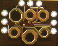
Figure 4 Photograph of the LNA with the modified shunt-Peaking load.
Design Example and Comparison
To demonstrate the practical viability of the proposed structure in CMOS technology, both the proposed topology and the conventional one have been applied to a 3.1 to 4.8 GHz wideband amplifier, based on a 0.35 µm standard CMOS process. Both circuits were optimized with the pads and on-chip spiral inductors analyzed with the MOMENTUM electromagnetic simulator.13
Figures 3 and 4 show the photos of the LNA with shunt-peaking load and the LNA with modified shunt-peaking load, respectively. As can be observed, the layouts are very similar with the exception of the LC inductor in the upper right corner. In both designs, the chip size, including the probe pads, is 949 × 760 µm. Each amplifier draws 17 mA from a 3.3 V supply.

Figure 5 Measured S-parameters for LNA with shunt-peaking load and modified shunt-peaking load.
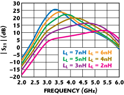
Figure 6 Gain simulation for different LL inductance using conventional shunt-peaking
The measured forward gain and input return loss of the amplifiers are shown in Figure 5 for frequencies from 2 to 6 GHz. For the proposed shunt-peaked LNA, the power gain is fairly flat at approximately 10 dB for frequencies ranging from 3.1 to 5 GHz. However, the same cannot be said for the conventional case, where a peak is evident. To flatten the insertion gain, the zero pole frequency should be placed as close as possible to the upper edge of the band by lowering LL. However, this entails a gain reduction, as can be seen in Figure 6, where the simulated S21 is plotted for different ideal LL inductors. As the inductance decreases, the flatness and bandwidth increase but the gain drops.

Figure 7 Measured noise figure for LNA with modified shunt-peaking and shunt-peaking load.
In both amplifiers, the input return losses remain the same, because both circuits share identical input matching circuits. As a consequence, the noise figure (see Figure 7) is also the same in both cases.
Conclusion
In this article, a novel wideband load configuration is presented. It is based on a conventional shunt-peaking resistor decoupled from the cascode stage through a capacitor. It offers the advantages of broadband operation and substantially higher gain flatness than a conventional shunt-peaking load. Its practical implementation in a standard low cost 0.35 µm process was discussed and verified. The presented results make the LNA design suitable for the 3.1 to 4.8 GHz UWB frequency range.
Acknowledgment
This work is partially supported by the Spanish Ministry of Science and Innovation (TEC2008-06881-C03-01), the Spanish Ministry of Industry, Tourism and Trade (TSI-020400-2008-71), and the “Programa de ayudas de Formación del Personal investigador, de la Agencia Canaria de Investigación, Innovación y Sociedad de la Información del Gobierno de Canarias y la cofinanciación y tasa de cofinanciación del F.S.E.”
References
- FCC, “Revision of Part 15 of the Commission’s Rules Regarding Ultra-wideband Transmission Systems,” FCC 02-48, First Report and Order, 2002.
- MB OFDM Alliance-SIG, “Multiband OFDM Phisical Layer Proposal for IEEE 802.15 Task Group 3a,” September 2004.
- A. Axholt, W. Ahmad and H. Sjoland, “A 90nm CMOS UWB LNA,” 26th Norchip Conference, Tallin, Estonia, November 2008.
- M. Ben Amor, M. Loulou, S. Quintanel and D. Pasquet, “A Dual Wideband CMOS LNA Design for the 4G of Wireless Application,” 2008 International Conference on Design & Technology of Integrated Systems in Nanoscale Era, Tozeur, Tunisia.
- B. Chi, C. Zhang and Z. Wang, “Bandwidth Extension for Ultra-wideband CMOS Low Noise Amplifiers,” 2008 IEEE International Symposium on Circuits and Systems Digest, pp. 968-971.
- X. Guan, Y. Jin and C. Nguyen, “Design of High Performance Compact CMOS Distributed Amplifiers with On-chip Patterned Ground Shield Inductors,” IEEE Electronics Letters, Vol. 45, No. 15, July 2009, pp. 791-792.
- M.M. Green, M.B. Pisani and C. Dehollain, “Design Methodology for CMOS Distributed Amplifiers,” 2008 IEEE International Symposium on Circuits and Systems Digest, Seattle, WA, pp. 728-731.
- A. Arbabian and A.M. Niknejad, “Design of a CMOS Tapered Multistage Distributed Amplifier,” IEEE Transactions on Microwave Theory and Techniques, Vol. 57, No. 4, April 2009, pp. 938-947.
- P.M. Roodaki, M.B. Kondori and P. Amiri, “Systematic Approach to Ultra-wideband Low Noise Amplifier Design in CMOS Technology,” 2008 IEEE International Conference on Semiconductors Electronics Digest, Johor Bahru, Malaysia, pp. 49-53.
- M. Yang, M. Ha, Y. Park and Y. Eo, “A 3 to 10 GHz CMOS Low Noise Amplifier Using Wire Bond Inductors,” Microwave and Optical Technology Letters, Vol. 51, No. 2, February 2009, pp. 414-416.
- A. Ismail and A.A. Abidi, “A 3 to 10 GHz Low Noise Amplifier with Wideband LC-Ladder Matching Network,” IEEE Journal of Solid-State Circuits, Vol. 39, No. 12, December 2004, pp. 2269-2277.
- T.H. Lee, The Design of CMOS Radio-Frequency Integrated Circuits, Cambridge University Press, New York, NY, 1998.
- J.R. Sendra, J. del Pino, A. Hernández, J. Hernández, J.
Aguilera, Andrés García-Alonso and A. Núñez, “Integrated Inductors Modeling and Tools for Automatic Selection and Layout Generation,” 2002 IEEE International Symposium on Quality in Electronic Design, San Jose, CA.