

Analog Devices has introduced four new Digital Variable Gain Amplifiers (DVGA): ADL5201 and ADL5202, which are IF DVGAs; and ADL5240 and ADL5243, which are RF DVGAs. These new DVGAs will enable the design of smaller base stations with multiple carrier capabilities for next generation wireless systems such as Long Term Evolution (LTE) systems.
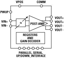
Figure 1 ADL5201 Block diagram.
The ADL5201 and ADL5202 DVGAs are optimized for use in IF sampling receivers. The ADL5201 (see Figure 1) is suitable for single-channel receivers while the dual-channel ADL5202 is suitable for use in main and diversity or MIMO receivers. For the most common IFs used between 70 and 300 MHz, both these devices exhibit minimum amplitude variations over frequency, allowing designers to choose an optimum IF for their design. With a gain range of 31.5 dB (-11.5 to 20 dB), these devices can be used to expand the dynamic range of high performance IF sampling receivers. In addition, a gain-control step size of 0.5 dB ensures that the full input range of the analog-to-digital converter (ADC) can be fully utilized.
The ADL5201 and ADL5202 DVGAs feature novel and flexible gain control interfaces. In addition to parallel and serial interface options, a novel up/down mode is also available. When operated in parallel mode, the 6-bit gain code can either be latched into a register or the register can be made transparent resulting in the gain following the code on the six gain control pins. In serial mode, the gain is set by clocking serial data into the devices’ serial to parallel interface (SPI), which also has a read back mode. In the serial mode, there is an additional fast attack mode where rather than setting the gain to a specific level, the gain can be changed by 2, 4, 8 or 16 dB step increments or decrements. The gain can also be changed using an up/down interface. This allows the gain to be incremented up or down in steps of 0.5, 1, 2, or 4 dB. The gain control interfaces of the IF DVGAs are designed to allow simple interfacing to ADCs from Analog Devices, such as the AD9643, which features over range detection. When the ADC is connected to an ADL5201 or ADL5202 up/down interface, over range detection at the ADC’s output port starts decreasing the gain until the ADC is no longer in an over drive condition.
The ADL5201 and ADL5202 provide outstanding linearity, with an output third-order intercept point (OIP3) of better than +50 dBm at the high end of the gain range at IFs up to 150 MHz. Another key feature of these devices is the low power mode, which reduces the supply current by 25 percent compared to the standard operating mode. Operating in the low power mode results in a moderate drop in linearity, but the mode can be switched on and off based on dynamic conditions in the receiver. For example, under normal receive conditions the low power mode could be used with the higher linearity mode turned on only when large in band blockers are present.
The ADL5240 and ADL5243 are high-performance RF DVGAs that operate over a broad frequency range of 100 MHz to 4 GHz. The ADL5240 integrates a DSA with a broadband, fixed-gain amplifier. The amplifier is internally matched and has a broadband gain of approximately 19.5 dB. The 6-bit DSA has 31.5 dB gain-control range, 0.5 dB step size and ±0.25 dB step accuracy over the entire frequency range. The DSA attenuation can be controlled by using either a parallel or serial interface mode. The DSA and amplifier in the ADL5240 can be wired for the attenuator to drive the amplifier, for transmit applications, or for the amplifier to drive the attenuator, for receive applications. The ADL5240’s +38 dBm OIP3 and 3 dB noise figure make the device attractive for both receiver and transmitter signal paths.
The ADL5243 provides an even higher level of integration. Along with a broadband amplifier and a 31.5 dB DSA, the ADL5243 includes a second amplifier. This allows the device to be configured in an amplifier-DSA-amplifier component lineup. When the three components are connected in the aforementioned configuration, they provide a cascaded gain of 29 dB when the DSA is set to minimum attenuation. The ADL5243’s final stage amplifier is designed to deliver highly linear output power with OIP3 of +41 dBm and is capable of driving directly into a base station power amplifier. Like the ADL5240, the DSA attenuation in the ADL5243 can be controlled either by a parallel or serial interface mode and support 0.5 dB step size with ±0.25 dB step accuracy.
The newly introduced RF and IF DVGAs from Analog Devices provide significant integration advantages with reduced system and cost complexity and will support and enable small footprint designs for next generation wireless systems.
Analog Devices Inc.,
Wilmington, MA
(978) 658-8930,
www.analog.com
RS No. 305