
The last decade has seen a great burst in wireless communication technologies and their commercial implementations. Until now, the third generation (3G) mobile networks (such as UMTS and cdma2000) and 3.5G mobile networks (such as UMTS/HSPA and CDMA 1xEvDO), which can deliver data rates up to several Mbps to individual users, have been deployed in many countries and adopted by more and more people. However, the pursuit for higher data rates never stops, and a number of wireless technologies are under development to meet future needs: Long Term Evolution (LTE) and WiMAX, both of which can support far higher data rates than existing networks. According to the definition of IMT-Advanced (4G) systems by the International Telecommunication Union (ITU), the next generation network should support data rates up to 100 bps for high mobility and approximately 1 Gbps for low mobility. Unfortunately, neither LTE nor WiMAX can fulfill these requirements. Currently, much work is going on to enhance these exiting standards in order to meet the requirements of the IMT-Advanced system.1,2 The roadmap of evolutions of various candidates toward the IMT-Advanced system is shown in Figure 1.3

Figure 1 Evolution of mobile technologies toward the next generation system.
To meet the requirement of the data rates defined in the IMT-Advanced system, the channel bandwidth will be up to 100 MHz. Moreover, the MIMO technique is needed to obtain higher channel capacity or spectrum efficiency. When the channel bandwidth approaches 100 MHz, RF designers have to face many challenges, both in the system scheme and the circuit design. It is known that the 6 × 6 MIMO configuration can provide more than 10 bit/Hz in the spectrum efficiency in many typical wireless channels without too much difficulty. In this article, a detailed description of the design of a high performance MIMO RF transmitter with a novel direct-conversion architecture is provided. The RF transmitter operates in the 3.45 GHz frequency band with 100 MHz channel bandwidth and excellent EVM and gain flatness performance. Experimental results are reported. The transmitter can support the 6 × 6 MIMO configuration and has been successfully used in an IMT-Advanced experimental network.
System Architecture
Compared to the conventional superheterodyne architecture, the direct-conversion solution has gained more and more attention and applications in various low-cost and compact wireless communication systems.4-6 Unlike the direct-conversion receiver, which has design challenges still needed to be resolved in order to achieve high performance, it is relatively easier to build a direct-conversion transmitter.7

Figure 2 System diagram of the direct conversion transmitter.
The transmitter reported utilizes a direct-conversion architecture illustrated in Figure 2. This diagram is just an abstract illustration and only essential components are outlined. Other necessary circuits, such as the control circuit, power supply circuit, etc., are omitted for brevity.

Figure 3 Architecture of the LO generator.
The configuration of the PLL is shown in Figure 3 and will be introduced later. As shown, the transmitter utilizes differential analog I/Q inputs, which are used not only to get a better signal-to-noise ratio due to common mode noise rejection, but also to suppress the even order distortions resulting from the nonlinearity of the quadrature modulator. The low pass filters following are used to further reduce the out-of-band emission level and aliasing products.
Next, the operational amplifiers can provide a certain DC offset, required by the inputs of most quadrature modulators. Usually these operational amplifiers should not provide very much gain since the baseband signal level is relatively large and even a few dB gain can saturate the modulator. In this transmitter, the input stage uses operational amplifiers of unit gain. The bandpass filter after the modulator suppresses the spurs resulting from the nonlinearity of the modulator. The transmitter works in the TDD mode, so it is important to switch off the RF amplifier and power amplifier as fast as possible when the receiving period is on, but the bypass capacitors necessary for the stability of the amplifiers always make this unpractical. To prevent the receiver from saturation or jamming by the power amplifier at the start of the receiver period, it is wise to use a RF switch, right before the RF driver amplifier together with the one before the antenna, both of which feature fast switch speed within 60 ns and thus provide enough isolation between the receiving and transmitting period quickly.
The Automatic Power Control (APC) is realized with digital attenuators, which can provide more than 60 dB attenuation control range in 0.5 dB steps. The required output power of the transmitter is 20 dBm. Considering the peak-to-average ratio of the transmitted signal, a MMIC power amplifier capable of 33 dBm output power at its 1 dB compression point is utilized. To further assure the linearity, the output IMD level is tuned and optimized when the output power is approaching 25 dBm.
Usually, special attenuation should be paid in the design of the PLL used in the direct-conversion architecture in order to avoid the LO pulling effect, which can seriously deteriorate the system performance. As briefly shown in Figure 3, the transmitter works on a carrier with an offset from the running frequency of the VCO. The offset is produced using a by 2 frequency divider fed by the VCO; the 3.45 GHz carrier is then obtained by mixing the output of the VCO with this offset. The bandpass filter is used to suppress the unwanted mixing products. The common reference clock of 10 MHz shared by the 6 × 6 MIMO system is produced either by an OCXO whose frequency can be precisely adjusted by the system AFC loop, or by the outside reference source, meanwhile bypassing the inside OCXO. This architecture is very flexible in a prototype system and capable of minimizing the frequency offset between the receiver and the transmitter, which can degrade the system performance especially when using an OFDM modulation scheme. Furthermore, the LO phase noise should be carefully optimized to achieve good system performance.8
Considerations of Broadband Operation
In the case of broadband operation, the performance of the quadrature modulator greatly determines the overall transmitter performance, such as the modulation accuracy indicated by EVM.9 Compared to the narrowband case, the amplitude and phase unbalance among the differential I/Q input channels becomes more serious and thus brings about the image product, which aggravates the system performance. Furthermore, almost every quadrature modulator in the market requires a DC offset at its differential I/Q input, the unbalance of which makes the elimination of the LO feed through problem more difficult.
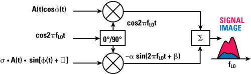
Figure 4 Simple model representing various unbalanced componets resulting in the image product.
Image product
The mechanics resulting in the image product can be clarified using a simple model shown in Figure 4. As illustrated, σ and α represent the amplitude unbalance and ε and β represent the phase unbalance. The image lies in the same frequency band as the signal, thus degrading the modulation accuracy. The lengthy development of the output signal equations can be found in the literature.7 In the case when OFDM is utilized, the up converted signal and its image are shown in Figure 5, in which the individual carrier and its image are drawn in the same color.

Figure 5 Up-converted signal and its image when using OFDM.
In reality, the amplitude and phase unbalances always exist in the differential I/Q channel, so the image product cannot be completely avoided. Of course, the unbalance of the LO path in the quadrature modulator can also result in the image product, but the influence is relatively smaller. Usually, the image product can be compensated in the baseband processing, such as adaptive adjustment of the amplitude and phase of the I/Q signal as part of the digital predistortion loop, or simply setting a fixed amplitude and phase offset.

Figure 6 The unadjusted image suppression.

Figure 7 The adjusted image suppression.
In the RF scenario, to alleviate the performance degradation caused by the image product, attention should be paid to the PCB layout process where the differential I/Q channels should be identical in their physical layout. In the tuning process, the level of the image product can be evaluated from the image to signal ratio, which can be measured using a spectrum analyzer. The unadjusted single tone output with its image product is shown in Figure 6. Then, capacitors on the order of several pF can be shunted to ground from the signal traces of the differential I/Q channels. The working of the capacitors results from their non-ideal parameters, which can be modeled as a complex impedance; the magnitude and phase of the baseband signal can then be slightly tuned. After carefully tuning, an image to signal ratio or image suppression below -35 dBc can be achieved throughout the working band. The improved image suppression is shown in Figure 7.
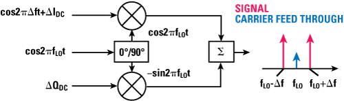
Figure 8 Simple illustration of the carrier feed-through problem.
Carrier Feed Through
The carrier feed through results not only from the DC offset unbalance among the I/Q differential inputs, but also from the LO leakage of the quadrature modulator. Usually the LO leakage is not a concern because it is very small in a MMIC quadrature modulator. The mechanics behind the carrier feed-through problem due to DC offset unbalance is illustrated in Figure 8. If a two-tone output is desired, the baseband I/Q signal can then be expressed by the following, with their corresponding DC offset:

According to the above equations, the component underlined in Equation 3 is the carrier feed-through product. The input DC offset levels can be slightly adjusted around the recommended common mode voltage required by the quadrature modulator to greatly reduce the carrier feed-through level. The circuit realizing the tuning function is shown in Figure 9. After iterative adjustment of the DC offset of the I/Q differential input, the carrier feed through to signal ratio or carrier suppression below -50 dB is easily achieved. The tuning result is shown in Figure 10.

Figure 9 Circuit realizing the tuning of the DC offset level using an operational amplifier.

Figure 10 The unadjusted carrier feed through (a) and the adjusted carrier feed through (b).
Measurement Results
The transmitter reported in this article is integrated together with the receiver into one single PCB board. The whole 6 × 6 MIMO system consists of six such transceiver modules as well as one control board, which acts as an interface to the baseband serial control signals, and one power supply board providing the DC-DC conversion from 48 to 6 V used by the transceiver. The 6 × 6 MIMO system equipped with six transceiver modules is illustrated in Figure 11.

Figure 11 The 6 × 6 MIMO RF transceiver.
The transmitter is tested with analog I/Q inputs from a vector signal generator. During the test process, it is convenient to divide the transmitter into three parts: modulator, driver and power amplifier, which can be tuned and tested individually. In the modulator test, the performance that is cared about is the modulation accuracy indicated by EVM. The LO phase noise should first be optimized by adjusting the setting of the synthesizer and the loop filter. After adjustments of the unbalance level mentioned before, the modulation accuracy can then be guaranteed. The resulting LO phase noise figure and the EVM of different modulation type are listed in Table 1, together with the image to carrier ratio and carrier feed through level. Due to the limited capability of the laboratory instruments, the maximum signal bandwidth that can be analyzed is 20 MHz.


A conventional S-parameter test is carried out in the testing of the driver and power amplifier. After careful tuning, the gain fluctuation is kept below 0.5 dB in each stage. An additional IMD test is also carried out to evaluate the nonlinearity of the power amplifier when the output level of 25 dBm is achieved. The results are listed in Table 2.

After individually testing of the different stages, the whole link is connected and tested. The overall performance, indicated by the EVM when the output level achieves the specified 20 dBm, is listed in Table 3.

Figure 12 Constellation diagram.

Figure 13 Error vector spectrum.
With help from the Agilent Open Laboratory in Beijing, China, the transmitter was tested with a baseband signal of 80 MHz modulation bandwidth, which was the maximum digital modulation bandwidth available from Agilent at that time. The results are shown in Figures 12 and 13. The channel 1 OFDM error summary is shown in Table 4.

Conclusion
The implementation of a broadband direct-conversion transmitter is reported. The considerations of system architecture are discussed in detail and the issues regarding the broadband working are illustrated. The transmitter was integrated in a 6 × 6 MIMO wireless prototype system capable of data rates up to 1 Gbps in a low mobility scenario.
Acknowledgment
This work was supported in part by NSFC under Grant 60621002 and 60702027, 60921063 and in part by the National 973 project 2010CB327400, by the National High-Tech Project under Grant 2008AA01Z223, 2008ZX03005-001 and 2009AA011503.
References
- M. Sauter, Beyond 3G - Bringing Networks, Terminals and the Web Together: LTE, WiMAX, IMS, 4G Devices and the Mobile Web 2.0, John Wiley, Somerset, NJ, 2009.
- H. Holma and A. Toskala, W-CDMA for UMTS: HSPA Evolution and LTE, John Wiley & Sons Inc., Somerset, NJ, 2007.
- J. Walko, “Mobile Operators Under Pressure in Barcelona—3GSM Report,” Picochip, EETimes Europe, February 19-March 4, 2007.
- M. Hotti, J. Kaukovuori, J. Ryynanen, K. Kivekas, J. Jussila and K. Halonen, “A Direct Conversion RF Front-end for 2 GHz W-CDMA and 5.8 GHz WLAN Applications,” 2003 Radio Frequency Integrated Circuits (RFIC) Symposium Digest, pp. 45-48.
- A. Abidi, “Direct-conversion Radio Transceivers for Digital Communications,” IEEE Journal of Solid-State Circuits, Vol. 30, No. 12, December 1995, pp. 1399-1410.
- M. Kawahima, H. Hayashi, T. Nakagawa, K.Nishikawa and K. Araki, “A 0.9 to 2.6 GHz Broadband RF Front-end for Direct Conversion Transceivers,” 2002 IEEE MTT-S International Microwave Symposium Digest, Vol. 2, pp. 927-930.
- Q.H. Gu, RF System Design of Transceivers for Wireless Communications, Springer, Secaucus, NJ, 2006.
- L.H. Li, F.L. Lin and H.R. Chuang, “Complete RF System Analysis of Direct Conversion Receiver (DCR) for 802.11a WLAN OFDM System,” IEEE Transactions on Vehicular Technology, Vol. 56, No. 4, Part 1, July 2007, pp. 1696-1703.
- M. Iglesias, “Understanding W-CDMA Modulation Quality Measurements,” Microwave Journal, Vol. 45, No. 12, December 2002, pp. 56-70.