
In the last decade, cellular mobile devices have undergone dramatic changes. What began as a mobile phone simply used for people to talk or text with one another has now turned into a handheld device that provides multi-functionality such as a phone, web browser, text messenger, camera, gaming unit, MP3 player, and many other useful functions to satisfy our need for information on-the-go. Not only do today’s mobile device users want all of these features included, they also want them readily available to them at all times, irrespective of time or location. This type of on-demand mobile technology requires compatibility of multiple frequency bands and modulation standards. This type of complex functionality, along with the consumer’s desire for smaller form factors, has placed great demands on mobile designers to deliver products at a lower bill of materials (BOM) cost and within record-breaking time to satisfy the market’s expectations generation over generation. Such stringent requirements have forced designers to undergo a change in the way that RF front ends are benchmarked. This article discusses some of these impacts and how a new approach can be embraced to enhance the consumer experience when using a feature-rich mobile device.
![]()
Figure 1 External stub antennas.
Readers who were in the industry several years ago can remember that voice was the primary driver for performance, and the most widely used modulation format was GSM/GPRS. Handset designs were much larger, with more printed circuit board (PCB) real estate dedicated to the RF front-end section, and performance was the primary focus of the project. The antennas were external to the handset, as depicted in Figure 1, taking the form of a stub or slider that pulled out and retracted with efficiencies that were much better than what a user can find in a handset today. Phones were designed to be operated in voice-only calls with the handset or mobile device held in a fairly predictable position relative to the user’s head. The consistency allowed the antenna to be designed in a fairly known environment that allowed for optimization of the design. This is still critical today since the power amplifier (PA) can be a significant drain on talk time, which is directly correlated to a user’s experience with a certain model of device as well as the company brand of mobile device. If the designer can optimize the current consumption in a real-world environment, the better positioned the mobile device is in the consumer market. The consistency of antennas and their real-world behavior has given handset designers the flexibility to optimize their design by impedance matching antennas and PAs in order to deliver the maximum amount of power as efficiently as possible.

Figure 2 PIFA antenna.
Mobile Devices: That was Then, This is Now
Fast forward a couple of years and the mobile device market has changed dramatically. Real estate is now dedicated to applications processors and components that are more focused on software applications than enhancing the consumer experience. Mobile devices are now designed with much smaller form factors and performance has been traded off in many cases to achieve these unique form factors. Handsets today have integrated patch or Planar Inverted F Antennas (PIFA) (illustrated in Figure 2) that in many cases are far less efficient to their predecessors. Even today, some handsets are now reverting back to a stub antenna due to the issues that many designers are facing. This performance versus form factor tradeoff directly impacts a consumer experience in the form of battery life, talk time and network availability since the antenna choices and their environment affect the PA.

Figure 3 VSWR performance of a PIFA antenna in a mobile device.
One example of how this affects PA performance is in the form of voltage standing wave ratio, or VSWR. Mobile devices today are operated in three basic configurations. Users talk on the mobile device with the handset next to the head in a conventional manner, out in front of their head using the speaker phone and in a free space environment where the phone is not held. These are just three scenarios in which the VSWR response of the antenna can change. In reality, there are numerous configurations determined by the position of the fingers and hand, but for simplicity this article is going to focus only on these three scenarios. The difference in performance of the antenna VSWR is illustrated in Figure 3.
These frequency responses illustrate the different VSWR requirements that the PA faces in a current generation handset. At the band edges, the PA will be exposed to VSWR ranges from 5:1 to 2:1 in this particular mobile device. The RX sensitivity is also affected due to the VSWR performance as well. Common practice used today by many handset designers for benchmarking RF front ends is measuring performance in a 50 ohm lab environment. This method is no longer practical in today’s designs due to the unpredictability of the impedances that are seen by the PA. A designer who wants to optimize his or her solution to provide the best talk time to the end user must begin to examine their RF front ends under VSWR conditions.
Standard governance boards such as 3GPP set the requirements for over-the-air (OTA) requirements. These requirements are usually much more relaxed than typical carrier requirements as they require more stringent OTA performance. A typical value a carrier may set for their mobile devices is -11 dB from conducted RF output power. In terms of the GSM 850 standard, this would equal a value of 22 dBm OTA requirement since conducted output power requirement is set to 33 dBm with -11 dB of loss due to antenna efficiency and propagation effects which are frequency dependent. These OTA requirements are directly applicable to the 50 ohm power if RF front ends are benchmarked and compared with these requirements in mind.

Figure 4 Current control block diagram.

Figure 5 Voltage control block diagram.
GSM Power Control Architectures’ Effects on Talk Time
The three different architectures most commonly used in the industry today for GSM mobile applications are current control, voltage control and power detection. A simplified block diagram of each of the three architectures is illustrated in Figures 4, 5 and 6.

Figure 6 Power detection block diagram.
Numerous articles have been published on the theory of these three architectures; therefore, this article will provide only a brief description as background. The current control architecture in Figure 4 is an indirect control scheme in which the current is monitored and held constant. This method relates current to power and provides a very good method of power control as long as the relation between current and power remains constant (which occurs only if the resistance of the load does not change). Power is controlled by adjusting the base bias of the amplifier controlling the gain, which results in power control. Figure 5 is an illustration of voltage control, which is very similar to current control in the sense that it is an indirect method relating voltage to power instead of current. This method—much like current control—works well as long as the resistance of the load remains constant and the relationship between voltage and power is maintained. The collector voltage is adjusted to control power instead of the base bias like in current control. The final architecture to be compared in this article is power detection, which is illustrated in Figure 6. In this method, power is detected by coupling a portion of the signal back to a detector that compares the output voltage and the reference voltage. The accuracy of this power control scheme is great as well and the mismatch performance is greatly dependent on the directivity of the coupler and the error in the feedback loop. The disadvantage of this architecture, however, is the added output loss of the coupler and the cost of the component, as it takes more circuitry to accomplish the power control function.
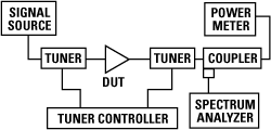
Figure 7 Load pull setup.
After reviewing a very simplistic view of basic power control architectures, one can focus on benchmarking the devices in such a way that reflects real-world performance and has a direct impact on the consumer satisfaction with talk time, battery life and call reception. First, to understand the real-world environment, the antenna performance must be characterized, as illustrated in Figure 3. As mentioned previously, the VSWR can range from 2:1 to 5:1, depending on the end user and how the phone is positioned. Based on these measurements, a good benchmark for comparison is determined to be a 3:1 VSWR. A VSWR of 3:1 is chosen as this will provide a good indication of part performance in the real world without providing unrealistic reflections back to the PA that may distort the results of the comparison. In order to characterize these products appropriately, a load pull must be performed where the designer has precise control over mismatch, phase angle and delivered power accuracy. Such a method is shown in Figure 7.

Figure 8 Current measurement into 3:1 VSWR with 50 Ω power set to 33 db.

Figure 9 Delivered power into 3:1 VSWR with 50 Ω power set up to 33 db.
After examining Figures 8 and 9, one can see that even though the power control function is achieved with different architectures, the performance in a real-world environment is very different. What does this mean and why is this so important? First of all, as previously discussed, what really matters is OTA performance, which is a direct correlation with delivered power. As Figure 9 shows, current control is the least desirable solution of the three for maintaining a constant delivered power into the load. There is almost 1.5 dB of difference between current control and power detection in the GSM 850 band. The disadvantage of the power detection scheme is that the current is allowed to increase, whereas the current is maintained reasonably well in the other solution. Although this would result in better talk time in this condition, in a real-world environment it would not.

Figure 10 Deltas in delivered power.
For example, if the mobile device is operated at 29 dBm, which is the power level that has the greatest probability in a GSM system, the base station would actually request that the handset increase its power level by moving from 29 to 31 dBm since the delivered power cannot be met at current power control level (PCL). This in turn would increase the current consumption and therefore decrease the talk time. Another aspect to consider is the current consumption advantages that can be realized. In a mobile device, if the current control scheme is providing enough delivered output power under these conditions to meet the carrier’s OTA requirements, then there is no need to be concerned about power into VSWR. Since the reduction of delivered power is good enough, substantial current consumption savings can be realized with a solution that provides better VSWR performance. In examining Figure 10, consider the following question: If the delivered power could be made equal between all solutions, what effect would this have on the end user?

Figure 11 50 Ω phasing target delta in current for equivalent delivered output power.
For voltage control and power detection, the 50 ohm calibration could be set 1 dB lower in power and still meet the equivalent delivered power. ETSI conducted specification specifies that for PCL 5 the power is 33 dBm ±2 dB under nominal conditions. This means that to meet conducted performance the mobile device can output a minimum of 31 dBm for PCL 5. Understanding the need for margin, the safest level that the mobile device should be calibrated to is 31.5 dBm. If more margin is desired, the designer could gain substantial current savings by phasing the mobile device to 32 dBm in a 50 ohm environment. How this correlates to 50 ohm performance is shown in Figure 11.
In Figure 11 the currents of the three solutions are compared versus output powers. This demonstrates that if the designer can achieve equal delivered output power to meet OTA requirements, then the current control solution would need to be calibrated for 33 dBm of output power compared to 1 dB less for power detection. This would result in 180 mA savings in the 50 ohm environment at full power, which can extend battery life and talk time. This current savings is realized without sacrificing any real-world delivered output power OTA performance. The other advantage to lower phasing targets is more margins to specific absorption rates (SAR) as well as lower harmonic generation since harmonic energy is much lower at 1 dB back-off from full power. This results in fewer emissions issues and faster time to market.

Figure 12 Delta in peak power.
If the designer is not interested in this approach and would like to have more output power, this can also be accomplished with a better VSWR tolerant device. The concern with higher output powers that every designer shares is the possibility of failing the SARs requirement for radiating energy in a multi-slot GPRS case. A much better, well-behaved VSWR tolerant device allows the handset to operate at higher power levels while still meeting SAR requirements under these conditions by limiting the amount of output power that is delivered in a low impedance state (see Figure 12).
Figure 12 illustrates that if a mobile device designer would like to optimize OTA performance, the phasing target could be increased in the mobile device 0.5 to 0.75 dB higher in the voltage and power detection solution compared to the current control. Phasing for higher targets statistically compromise SAR performance. As Figure 12 shows, however, the peak power swings are now equal for all three solutions, and the 50 ohm set power is much higher than the current control solution. This allows the designer to develop a superior product compared to the competition when compared at the carrier for OTA capabilities.
The final consideration is the tradeoff between transmit (TX) and receive (RX) performance and the ability to customize performance based on region. From Figure 3, the VSWR plot of a mobile antenna, there is room to shift the tuning to trade off TX performance for RX performance, if desired. Examining the purple trace, in the case where the phone is head loaded, one can see that if the GSM 850 TX and RX performance was degraded slightly by shifting the frequency response higher in frequencies, then the GSM 900 RX VSWR would actually improve. Having a VSWR tolerant TX path can allow the designer to have the flexibility to make the tradeoffs between the parameters that are most important in his or her particular design.
In conclusion, the importance of benchmarking solutions under mismatch conditions needs to be seriously considered. This method opens a new way of thinking that exposes designers to tradeoffs that can be made at the system level that may have not been considered before. Only examining solutions based on 50 ohm lab testing can and will cause misconceptions on selecting the right architecture for one’s design. In Figure 10, it is clear that almost all three solutions can perform the function and are very similar in performance. Although this is true in the 50 ohm environment, it is not the case in real world application. Considering OTA performance can result in greater flexibility for the designer to customize their product for better current consumption, high OTA power, or RX performance. All of these options are revealed if the designer is open to a new way of benchmarking RF front ends and making decisions that truly affect consumer satisfaction in terms of fewer dropped calls and longer battery life. As the end consumer experience improves, so does the brand image of that particular mobile device, which results in greater demand from consumers and higher adoption rates by the carriers.