
Solid-state switches based on high electron mobility transistors (HEMT) can be fabricated with a variety of different semiconductor technologies, usually selected on the basis of performance requirements. Such solid-state switches have been used successfully as control devices for transmitter and receiver switching functions in various digital communications systems. In these systems, HEMTs can be used as the signal control element connecting the transmitter and receiver subsystems to the antenna. The choice of material is dictated by the material’s critical breakdown field, its saturation drift velocity and its thermal conductivity. GaAs has for a long time been considered the most important material for digital applications. GaAs- and InP-based HEMT switches offer high isolation, low insertion loss and high switching speed1 but are limited in power-handling capabilities due to their modest critical breakdown fields. As a promising high power alternative, the wide band-gap, AlGaN/GaN HEMT might be used for the realization of microwave control and amplification functions.2
In recent years, satellite communication systems employing digital modulation schemes, increased channel capacity, high transmit power and extremely low receiver sensitivity have put into question the linearity of passive components.3,4 Even very low level multi-tone intermodulation products generated by switches can seriously degrade the efficiency of a system. A high quality microwave switch is a key building block of a radio frequency transmitter. It is well known that if the transmitter amplifiers and attendant switching functions are not extremely linear, amplitude modulation (AM)-to-AM and AM-to-phase modulation (PM) conversion can cause serious deterioration of the bit error rate (BER) and an increase in inter-symbol interference (ISI). Deterioration in communication link performance is mainly related to nonlinear noise effects in the RF sections of transmitter and receiver systems. The effects of these sources of noise or interference are increased by the nonlinear behavior of the transmitter RF power amplifier and the transmit switch. The nonlinear behavior of the HEMT used in a control mode will cause the introduction of unwanted signals into the circuit, creating harmonic or intermodulation products that can adversely affect system performance. In the past five years, several groups have concentrated their efforts on small- and large-signal modeling of HEMT control devices.5–7 Modeling the distortion properties has received little attention. In this article, in addition to the comparison of the performance for control functions in high frequency circuits, especially for those applications requiring relatively high power-handling capabilities, the nonlinear distortion characteristics of switches based on three different technologies are discussed and related to the problem of optimizing RF transmitter linearity. The effects of temperature on the performances of GaAs- and GaN-based control devices are also presented. This is carried out by considering the insertion loss, isolation and broadband cut-off frequency over a wide temperature range.
Switch Small-signal Characteristics
GaN is a wide band-gap semiconductor material with a high critical breakdown field, high saturation drift velocity and good thermal conductivity compared to GaAs and InP materials (see Table 1). It offers more than twice the band-gap energy of InP and GaAs materials, with more than three times the thermal conductivity of GaAs (implying much better power-handling capability). To evaluate the three semiconductor materials, a HEMT device structure was selected as optimum for high frequency switching and control functions.

The resistances and capacitances forming the HEMT equivalent circuit can be subdivided into two-state configurations. For most control applications and frequencies of most interest, the on-state impedance is primarily resistive, while in the off-state the impedance is primarily capacitive (see Figure 1). The modelled capacitances and resistances can be combined to form an equivalent circuit that would represent the two states of the HEMT control device. Note that the impedance in both states is estimated using the same techniques outlined in References 5, 6 and 7.

Fig. 1 HEMT control device in high impedance "off-state" (a) and in low impedance "on-state" (b).
The key figures of merit of a switch include insertion loss, isolation and power-handling capability. The on-state resistance (RON) and off-state capacitance (COFF) are the dominant factors determining the switch insertion loss (IL) or isolation (ISO), depending on the HEMT connection to the transmission line. The insertion loss measures the high frequency power loss through an RF switch when it is turned on. The isolation characterizes the RF power attenuation when the switch is turned off.
These two important switch parameters may be written in the SPST shunt configuration as

where
ZC = characteristic impedance
In the series SPST configuration, the two important switch parameters are given by

Finally, both on-state resistance and off-state capacitance are the key equivalent circuit elements used in characterizing broadband HEMT switches.
Figures 2 and 3 show the computed insertion loss and isolation as functions of gate voltage at a frequency of 1 GHz for three different technologies and with a gate periphery of 200 mm. The model used for the RON and COFF calculations is described in a previous work,4 with the simulated device structure of the same dimensions as the AlGaN/GaN device model. The impurity concentration of the AlGaAs, InGaAs or AlGaN and GaAs, InP or GaN layers are 6•1018cm–3 and 1•1013cm–3, respectively.

Fig. 2 Shunt-connected switch losses versus gate voltage at 1GHz.

Fig. 3 Series-connected switch losses versus gate voltage at 1 GHz.
A significant dependence of the extracted losses on Vg is observed. When the gate voltage decreases toward the threshold voltage (–0.1 V for InGaAs/InP, –0.46 V for AlGaAs/GaAs and –1.04 V for AlGaN/GaN), the loss decreases and increases rapidly in shunt and series configurations, respectively. This is in good agreement with the previous published results7 on modeling and measuring the AlGaN/GaN HEMT. In the gate voltage range greater or lower than the threshold voltage, the loss is rather flat, which is a good evaluation of the insertion loss and isolation in both configurations. For the shunt-connected switch, the InGaAs/InP HEMT switch presented a small variation on the level of insertion loss compared to the other technologies, but demonstrated an increase in isolation of 4 dB over the GaAs-based HEMT and 9 dB over the GaN-based HEMT switches due to the lower on-state resistance. The converse is true in the series case, where the isolation is approximately constant. The insertion loss of the three technologies is low, due the low on-state resistances of InGaAs/InP, AlGaAs/GaAs and AlGaN/GaN HEMT switches.
The broadband cut-off frequency figure of merit can be defined as

Switch Large-signal Characteristics

Fig. 4Shunt HEMT switch configuration.
The power characteristics of each technology in microwave control applications were also investigated in order to determine their power-handling capability. In order to define the insertion loss and isolation in a large-signal environment, a simple equivalent circuit of the shunt HEMT switch was used (see Figure 4). For a broadband HEMT switch, the power-handling is dependent on the gate bias circuitry. For gate voltage control isolation, the device is usually biased with a large gate bias resistance RGG or a resistor incorporated monolithically in the gate. The variations of shunt-connected HEMT isolation and series-connected HEMT insertion loss with the input power level at 1 GHz for three different technologies are shown in Figures 5 and 6, respectively. The effect of input power on the isolation and insertion loss is presented under on-state biasing conditions (Vg = +1 V). For the InP- and GaAs-based HEMT switches, there are strong degradations of isolation and insertion loss with increasing levels of input power higher than 0 and +3.5 dBm, respectively. Compared with the AlGaN/GaN HEMT switch, the same phenomenon occurs at power levels higher than +15 dBm due to the wide band-gap of the GaN material. This result shows the feasibility of using AlGaN/GaN HEMTs for high power microwave control.

Fig. 5 Power dependence of the isolation of a HEMT shunt switch with Vg=+1 V, F=1 GHz and ZL = 50?

Fig. 6 Power dependence of the insertion loss of a HEMT series switch with Vg=+1 V, F=1 GHz and ZL = 50?
Distortion Properties
In addition to the small- and large-signal modeling, a nonlinear model applicable to RF and microwave frequencies is necessary to determine the distortion characteristics of the HEMT. The basic circuit for the model is shown in Figure 7. It is a HEMT connected in series between a generator (VS, ZSG) (power amplifier) and a load (ZL) (antenna). The gate bias resistor RG is used to ensure that the gate is AC isolated from the ground and the RF path at all frequencies. A DC voltage (VCTRL) is applied to the gate to effect the switching action. In the circuit, ZSG = ZL = ZC, where ZC is the characteristic impedance of the transmission lines (LT1 and LT2), which is assumed to be 50 ?.
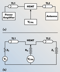
Fig. 7 Series-connected HEMT used in a transmitter as a control device (a) and a simplified representation (b).
To understand the distortion generated in HEMT switches, a nonlinear current-voltage relationship, IDS–VDS can be written as

where ?n terms describe the linear (n = 1) and nonlinear (n > 1) behavior of IDS and include the effect of the gate bias voltage VGS and the gate bias circuitry. Figure 8 shows a simple AC equivalent circuit model for the HEMT operating in a control mode, where ZS = 1/j?CS, ZD = 1/j?CD, ZL is the parallel combination of RGG and CGS or CGD and ZG is the parallel combination of RG and CG. The resistance RGG represents the gate leakage components.

Fig. 8 Simplified AC equivalent circuit of the series-connected HEMT.
The I-V characteristics of the HEMT are strongly influenced by the field dependent mobility of 2DEG. Using this approximation in Equation 4, the nonlinear drain-source current can be written as8

where
?LP = m0 only at low field conditions
VGS0 = DC control component
vGS = AC component caused by the gate leakage
IDsat is the drain current iDS at saturation, which occurs at an approximate value of VDS of (VGS0 – Voff), where Voff is the turn-off voltage.
In order to introduce the frequency dependence of the gate bias and leakage circuit, a parameter g was introduced,8 which describes the relationship between uGS and uDS and can be written as8
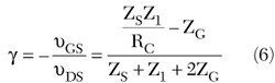
where
ZS = 1/j?CS
ZD = 1/j?CD
Z1 = parallel combination of RGG and CGS or CGD
Using Equation 5, the first three coefficients an of Equation 4 may be written as

where
?n (n=1,2) = mobility expansion coefficient
The discussion of the distortion in AlGaN/GaN HEMT switches will be limited to second- and third-order distortion intercept points (IP2 and IP3, respectively), which are of the most interest for microwave design purposes. For a single HEMT in a single series-connected configuration circuit as shown previously, the second- (IP2) and third-order (IP3) intercept points were computed using the equations9
The simulated device structure has a gate length of 0.25 ?m; the source-to-drain distance is 2 mm. The values of CGS, CGD and RG are 0.5 pF, 0.5 pF and 5 k?, respectively. Figure 9 shows the frequency dependence of IP3 of a HEMT switch for three different technologies with a turn-off voltage of –1.5 V and saturated drain current of 300 mA. The results show that the distortion intercept point is higher (less distortion) at low frequencies, especially for GaN semiconductor material due to its lower mobility and because in the HEMT, the gate-drain and gate-source circuit couples AC voltage to the gate, causing the 2DEG sheet density to vary with the applied signal. At low frequencies, the 2DEG sheet carrier density is somewhat higher than at higher frequencies with a corresponding slight decrease in nonlinearity, giving rise to the decrease in intercept point with increasing frequency. Also, the third-order distortion intercept point in the AlGaN/GaN technology is higher than its AlGaAs/GaAs and InGaAs/InP counterparts by about 23 and 29 dB, respectively. These differences are due to the higher saturation velocity and lower mobility in this device. A similar frequency dependence of the second-order intercept point was observed.

Fig. 9 Comparison of the third-order distortion intercept point (IP3) for the three different series HEMT switch technologies.
Temperature Effects
As GaAs and GaN technologies are the most used in power communications systems under high power conditions, a comparative study of the variation of their performance has been performed over a wide range of temperatures. The variation of the low field sheet resistivities, and HEMT capacitances and resistances forming the equivalent circuit with temperature are caused by the temperature effects on the electron mobility, saturated electron velocities, dielectric constant in GaN or GaAs, specific contact resistance and the barrier height between the metal gate and the AlGaN or AlGaAs layer. Appendix A presents the detailed temperature equations used in the calculations. Figure 10 shows the temperature effects on the broadband cut-off frequency, calculated with a gate periphery W = 200 mm for GaAs and GaN technologies. The dependence of the cut-off frequency on temperature in GaN material is smaller than its GaAs counterpart. When the temperature varies from –25° to +150°C, the broadband cut-off frequency decreases from 445 to 340 GHz in GaAs technology. Conversely, it is approximately constant in the AlGaN/GaN device due to the slight dependence of on-state resistance and off-state capacitance on temperature. This is in accordance with previously published results3 — a GaN-based switch can operate at temperatures above 140°C without degrading the switching speed performance.

Fig. 10 Broadband cut-off frequency versus temperature.
The variations of the series-connected HEMT insertion loss and shunt-connected HEMT isolation with the input power level and at three different temperatures, under on-state biasing conditions (Vg = +1 V) for the two technologies (GaAs, GaN), are presented in Figures 11 and 12, respectively. There are small degradations of isolation and insertion loss with increasing temperature for both switch configurations in the two technologies. The changes become approximately 1.2 dB for isolation and 0.1 dB for insertion loss when the temperature varies from 0° to 100°C in GaAs technology. The same changes were observed over a wider range of temperature in a GaN-based HEMT switch due to its wide band-gap energy. This result shows the feasibility of this device in some applications such as satellite systems where the environment conditions are hostile.

Fig. 11 Losses in a GaAs-based switch at different temperatures at Vg = +1 V; (a) shunt-connected HEMT isolation and (b) series-connected HEMT insertion loss.

Fig. 12 Losses in a GaN-based switch at different temperatures at Vg = +1 V; (a) shunt -connected HEMT isolation and (b) series-connected HEMT insertion loss.
Table 2 summarizes and compares the cut-off frequency, isolation, insertion loss and IP3 of the different microwave and RF control technologies. The cut-off frequency is estimated at a gate bias voltage of –2 V (COFF) and +2 V (RON) and at two different temperatures. It should also be noted that insertion loss and isolation are calculated at a power level of +20 dBm.

Based on the small- and large-signal characteristics, the distortion properties and the temperature effects comparisons, for low noise applications, an InP-based HEMT switch offers the best choice for optoelectronic switching functions, which require compatibility with InP-based optical devices and operating speeds of 40 Gbps and above. If high frequency operation is required, such as in digital communications systems, GaAs technology devices offer the best choice due to their high cut-off frequency and power performance. Finally, because a high power function is characterized by parameters such as power compression and third-order intermodulation, the most mature technology for this purpose is the GaN technology. The results show the feasibility of this technology for high power microwave control and indicate that the future is bright for this technology in satellite switching applications.
Conclusion
In this article, the performances of InP-, GaAs- and GaN-based HEMT switches are reviewed and discussed in the context of their suitability for microwave control applications. The results show that in high frequency switching operation, GaAs and InP technologies offer the best choice due to their high cut-off frequencies. On the other hand, due to the high breakdown voltage, high saturated velocity and low mobility, AlGaN/GaN HEMTs offer lower distortions and higher power-handling capabilities, where the degradation of their performances occurs at a power level up to +15 dBm. Compared with the InP- and GaAs-based HEMT switches, the same phenomenon occurs at the power levels of 0 and +3 dBm, respectively. The results indicate that the future is bright for the GaN technology in switching applications.
References
1. J.L. Cazaux, D. Pavlidis, G.I. Ng and M. Tutt, “A HEMT Monolithic Double Channel Attenuator with Broadband Characteristics and Wide Dynamic Range,” 18th European Microwave Conference, September 1988, pp. 999–1004.
2. E. Alekseev, Shawn S.H. Hsu and D. Pavlidis, “Broadband AlGaN/GaN HEMT MMIC Attenuators with High Dynamic Range,” Proceeding of the 30th European Microwave Conference, Paris, France, October 2000.
3. M. Kameche, “Temperature Effect on the GaN-based HFET for Microwave and RF Control Applications,” Second IEEE International Conference on Signals, Systems, Decision & Information Technology SSD’2003, Sfax, Tunisia, March 26–28, 2003.
4. M. Kameche and M. Bekhti, “Comparing High Frequency Control Devices,” Microwaves & RF, March 2003, pp. 53–61.
5. N. Jain and R. Gutmann, “Modeling and Design of GaAs MESFET Control Devices for Broadband Applications,” IEEE Transactions on Microwave Theory and Techniques, Vol. 38, No. 2, February 1990, pp. 109–117.
6. N.V. Drozdovski, R.H. Caverly and M.J. Quinn, “Large-signal Modeling of Microwave Gallium Nitride-based HFETs,” Proceedings of the Asia-Pacific Microwave Conference, Vol. 1, Taipei, Taiwan, December 3–6, 2001, pp. 248–251.
7. R.H. Caverly, N.V. Drozdovski and M.J. Quinn, “Gallium Nitride-based Microwave and RF Control Devices,” Microwave Journal, Vol. 44, No. 2, February 2001, pp. 112–124.
8. R. Caverly and K.J. Heissler, “On-state Distortion in High Electron Mobility Transistor Microwave and RF Switch Control Circuits,” IEEE Transactions on Microwave Theory and Techniques, Vol. 48, No. 1, January 2000, pp. 98–103.
9. R. Caverly, “Distortion in Broadband Gallium Arsenide MESFET Control and Switch Circuits,” IEEE Transactions on Microwave Theory and Techniques, Vol. 39, 1991, pp. 713–717.
10. Atlas User’s Manual (device simulation software), Silvaco Inc., Version 1.5.0, 1997.
11. J.S. Blakemore, “Semiconducting and Other Major Properties of GaAs,” Journal of Applied Physics, Vol. 53, 1982, pp. 123–181.
12. R. Anholt and S. Swirhum, “Temperature Dependence of GaAs MESFET Equivalent Circuits,” IEEE Transactions on Electron Devices, Vol. 39, September 1992, pp. 2029–2036.
13. A.V. Dimitriev and A.L. Oruzheinikov, “The Rate of Radiative Recombination in the Nitride Semiconductors and Alloys,” MRS Internet Journal of Nitride Semiconductors, Res. 1, 46, 1996.
Mohamed Kameche received his diploma degree in electrical engineering and his master’s degree in signal and systems from the University of Tlemcen, Algeria, in 1998 and 2001, respectively. From 1998 to 2001, he taught in the department of electronics at the University of Tlemcen. He is currently with the National Centre of Space Techniques (CNTS), Arzew, Oran, Algeria. His research interests include temperature effects on RF and microwave devices and package modeling for microwave circuit applications.
Nikolai Drozdovski received his diploma in electrical engineering and his candidate of technical science degree in microelectronics from the Moscow Power Engineering Institute (Technical University), Russia, in 1983 and 1993, respectively. He is currently with the Components Laboratory at ESA/ESTEC, The Netherlands. He has authored or co-authored more than 20 journal papers, 35 conference presentations and 10 patents. His main research interests include RF and microwave control devices and semiconductor components such as PIN diodes, MESFETs and HFETs.
| Appendix A: |
| For GaN material, the electron low field mobility is modeled as a function of the impurity concentration N and temperature T using10
where ?1 = 15 cm2/Vs
where the quoted value of s is usually equal to 2.3.11 For modern FETs, with doping concentrations greater than 1017 cm–3, the power law factor s is expected to be less than 0.5 with an uncertainty of ±0.1.
For GaAs material, the saturation velocity is modeled using a semi-empirical parameter
where ?sat is between (–1 and –2.5) × 10–3/°C. The dielectric constant in GaN varies as
where be is the temperature coefficient (TC). It was assumed to be equal to 1 × 10⁻⁴/°C for GaN, GaAs and other III-V materials.12 Finally, temperature variation of the threshold voltage, given by Equation A6,7 is derived from the temperature effects on the barrier height between the gate and the AlGaN or AlGaAs layer, the dielectric constant and the conduction-band discontinuity.
where ND = concentration in AlxGa1–xN The change in the barrier height and the conduction-band discontinuity with temperature is consistent with the temperature variations of the band-gap energy given by13
where ? = –0.939 × 10⁻³ eV/K2, ? = 772 K and
with the bowing parameter ? = 0.98 eV. The fact that the AlGaN or AlGaAs dielectric constants have a TC equal to 1 × 10⁻⁴/°C indirectly affects the threshold voltage of the HEMT. |


