
The demand for a signal source with high stability and low phase noise increases in microwaves, millimeter-wave communications and radar systems. High frequency signal sources can easily be obtained by multiplying low frequency signals that have relatively high stability and low phase noise. In general, however, frequency multipliers include some unwanted fundamental and harmonic frequency components. When a multiplier operates with other microwave circuits such as mixers and amplifiers, for example, serious problems may occur due to the undesirable frequency components. In order to suppress the fundamental frequency component (fo), a quarter-wavelength open stub or a balanced multiplier structure can be used, although these methods generally have the limitation of suppressing the unwanted harmonics by only 25 dB.1,2 A balanced frequency doubler using an input balun can be used to cancel the fundamental. However, the cancellation characteristics depend on the phase unbalance of the balun and the uniformity of the transistors. Typically, a 20 dB fundamental rejection at microwave frequencies is obtained.3 Another way to diminish the fundamental and unwanted harmonic components is to use bandpass filters, although the insertion loss of the bandpass filter attenuates the multiplied signal level as well. In addition, it is not easy to make high Q-factor bandpass filters in monolithic microwave integrated circuits. The design of a fully monolithic frequency doubler is very difficult.
In this article, a novel frequency doubler that suppresses fundamental and unwanted higher order harmonic components is described. The proposed doubler is composed of a feedforward structure, which is widely used in linear power amplifiers, and a defected ground structure (DGS) realized by etching a few dumbbell shaped patterns on the ground plane of the microstrip line.4 Several applications using DGS to design a coupler, filter and power amplifier have already been presented.5–7 The feedforward loop suppresses the fo signal and the DGS suppresses the other unwanted harmonic components more effectively than by previous methods.
Theory
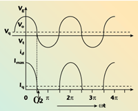
Fig. 1 Output current for a conduction angle.
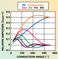
Fig. 2 Amplitude comparison of the fundamental and harmonic componenets versus conduction angle.
The output current waveform versus the input voltage of a transistor can be described according to the bias condition or conduction angle. Figure 1 shows the output current for a given conduction angle. The DC current and harmonic signals at the bias condition are estimated by using averaging and correlation between drain (or collector) current and the nth harmonic, as shown in Equations 1 and 2, where ? is the conduction angle of the input signal and Imax is the maximum allowable current.8 Figure 2 shows the amplitude comparison of the DC current, the fundamental and the harmonic current components versus conduction angle.

The amplitude of the second harmonic is maximum when a is set at approximately 120°. Therefore, the bias point for a frequency doubler should be selected in the vicinity of pinch-off, between class B and C. Once the bias is determined, the input and output ports have to be matched at the fundamental frequency (fo) and at the frequency of the second harmonic signal (2fo), respectively, to maximize the 2fo output.
Figure 3 shows the proposed frequency doubler, which uses a feedforward structure to suppress fo, and a DGS microstrip line to attenuate the other higher order harmonics. The feedforward structure is widely used to remove the intermodulation distortion in power amplifiers. It has a wide operating frequency band and hardly oscillates because there is no feedback path. In this article, the first loop of the feedforward structure is used to suppress fo. Because active multipliers attenuate fo theoretically, fo can be suppressed further by adjusting the coupling coefficient of the couplers, which are located before and after the multiplier, and the phase of the variable phase shifter.9 To have perfect cancellation of fo, the magnitude and phase of the two signals must be equal and out-of-phase at the output coupler of the feedforward structure. The coupling coefficients of the input and output couplers are adjusted to match in magnitude, and the phase of the variable phase shifter is adjusted to obtain the out-of-phase condition between the two paths.
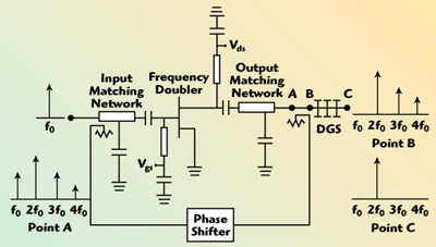
Fig. 3 Block diagram of the proposed frequency doubler.
The DGS pattern under the microstrip line produces an additional equivalent inductance and an increase in characteristic impedance. In conventional microstrip lines, the line width becomes extremely narrow as the required line impedance increases. However, in the microstrip line with DGS, the line width is broader than that of the standard microstrip line for the same characteristic impedance, because the additional inductance results in a highly increased characteristic impedance. The broadened width of the DGS microstrip line can be understood as an increased equivalent capacitance, which plays an important role in raising the phase constant and slow-wave effects.7 In this work, the DGS microstrip line is used to suppress the higher order harmonics above the third.
Figure 4 shows the layouts of a standard microstrip line and DGS microstrip line. The substrate is RT/duroid 5880 with a dielectric constant of 2.2 and a thickness of 31 mils. The DGS cell dimensions are: a = 4 mm, b = 3.5 mm, dc = 9.3 mm, g = 0.5 mm, w = 2.38 mm and wdgs = 4.37 mm. It is possible to control the electrical characteristics by adjusting the DGS cell parameters.
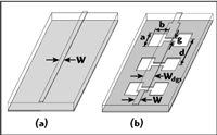
Fig. 4 Layouts of (a) a strandard microstrip and (b) a DGS microstrip.
Figure 5 shows the measured S11 and S21 of the DGS microstrip line. The DGS microstrip line has characteristics that are just like those of low pass filters. The cut-off frequency is around 4 GHz, the insertion loss is 0.4 dB at 3.74 GHz and the attenuation at 5.55 GHz is more than 23 dB.
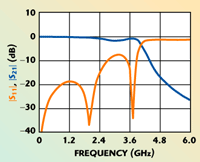
Fig. 5 Measured characteristics of the DGS microstrip line.
Experiment and Measured Results
In order to show the validity of the proposed doubler, a frequency doubler was designed to multiply a 1.87 GHz fundamental signal to produce a frequency output at 3.74 GHz. The selected transistor was an ATF10136 MESFET. The drain and gate bias voltages are set to 1.2 and –1.25 V, respectively, for a near pinch-off voltage operating region between classes B and C. The matching conditions for the input and output networks were determined by using a load-pull method and were implemented by simulation with Agilent ADS.
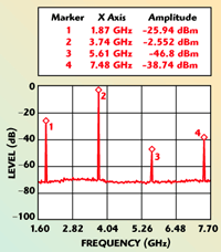
Fig. 6 Measured spectrum of the conventional frequency doubler.
Figure 6 shows the measured output spectrum of a conventional single-ended frequency doubler. The spectra of the conventional doubler show the 2fo output signal as well as the fairly large fo and other higher order harmonics. It has a conversion loss of 2.55 dB and a fundamental suppression of –25.94 dB when the input fundamental signal is 0 dBm. Figure 7 shows the measured data of the frequency doubler using the feedforward structure without DGS. The measured fundamental suppression is 42.2 dB higher than for a conventional doubler. Figure 8 illustrates the measured output spectrum of the proposed frequency doubler including the feedforward structure and the DGS microstrip line, where the proposed frequency doubler is fabricated on the same PCB. For the same input power, the output power at 2fo is –3 dBm with harmonic suppressions greater than for the conventional doubler by 42.9 dB, 19.2 dB and 29.7 dB at fo, 3fo and 4fo, respectively. Table 1 summarizes the output spectrum characteristics of several frequency doubler structures.

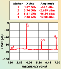
Fig. 7 Measured spectrum of the frequency doubler having the feedforward structure only.
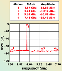
Fig. 8 Measured spectrum of the proposed frequency doubler having the feedforward structure and DGS microstrip line.
Figure 9 shows the fundamental signal suppression characteristic from the feedforward structure as a function of frequency. Although the fundamental is suppressed by about 42.9 dB at the center frequency, only 14 dB suppression is obtained at the frequency band edges. For a wider band suppression, a constant conversion loss at fo and a flat group delay must be obtained.
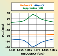
Fig. 9 Fundamental signal output suppression from the feedforward structure as a function of frequency.
Figure 10 shows the conversion loss as a function of frequency. The conversion loss at 3.74 GHz is –2.9 dB and the conversion loss variation over a 100 MHz range is ±1.73 dB. Figure 11 shows the conversion loss as a function of input power level. From the measured results, the 1 dB compression point of the fabricated frequency doubler is about –1.5 dBm.

Fig. 10 Conversion loss as a function of frequency.
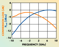
Fig. 11 Conversion loss and output power at 2f0=3.74 GHz versus input power at f0=1.87 GHz.
Figure 12 shows the phase noise characteristics of the input and output signals. The measured phase noise at 2fo is –97.51 dBc/Hz (at 10 kHz offset) when that of the fo signal is –101.3 dB, the 3.8 dB phase degradation is better by 2.2 dB than the theoretical phase degradation condition expressed by 20log(2) = 6 dB. It is believed that this result is due to the effective elimination of the fundamental and higher order harmonic signals. The DGS microstrip line is operated as a harmonic short. The phase noise of the proposed frequency doubler is improved over that of a conventional one.
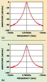
Fig. 12 Phase noise of (a) input signal and (b) output signal.
Conclusion
A new design technique for a frequency doubler was proposed to obtain signal sources that have high stability and low phase noise. The fundamental frequency signal was suppressed by using a feedforward structure, and the unwanted higher order harmonics were removed with a DGS structure. The measured suppressions of the fundamental, and third and fourth harmonic components for the proposed doubler were 42.9 dB, 19.2 dB and 29.7 dB, respectively, over those of a conventional frequency doubler. It is believed that the proposed frequency doubler can be integrated in monolithic integrated circuit form because the fabricated frequency doubler consists of a transistor, diodes (in the phase shifter) and hybrid circuit elements. It is also expected that the proposed frequency doubler would contribute significantly to the improvement of the quality of communications without the use of high Q bandpass filters.
References
1. D.G. Thomas, Jr. and G.R. Branner, “Optimization of Active Microwave Frequency Multiplier Performance Utilizing Harmonic Terminating Impedances,” IEEE Transactions on Microwave Theory and Techniques, Vol. 44, No. 12, December 1996, pp. 2617–2624.
2. S.P.O. Bruce, F.J. Beiwanger, J.F. Luy and U. Erben, “Design and Realization of a Millimeter-wave Si/SiGe HBT Frequency Multiplier,” IEEE Transactions on Microwave Theory and Techniques, Vol. 46, No. 5, May 1998, pp. 695–700.
3. S.A. Mass, The RF and Microwave Circuit Design Cookbook, Artech House Inc., Norwood, MA, 1998.
4. C.S. Kim, J.S. Park, D. Ahn and J.B. Lim, “A Novel 1-D Periodic Defected Ground Structure for Planar Circuits,” IEEE Microwave and Guided Waves Letters, Vol. 10, April 2000, pp. 131–133.
5. J.S. Lim, C.S. Kim, J.S. Park, D. Ahn and S. Nam, “Design of a 10 dB 90° Branch Line Coupler Using Microstrip Line with Defected Ground Structure,” Electronics Letters, Vol. 36, No. 21, October 2000, pp. 1784–1785.
6. D. Ahn, J.S. Park, C.S. Kim, J. Kim, Y. Qian and T. Itoh, “A Design of the Low Pass Filter Using the Novel Microstrip Line with Defected Ground Structure,” IEEE Transactions on Microwave Theory and Techniques, Vol. 49, No. 2, January 2001, pp. 86–93.
7. Y.C. Jeong, S.G. Jeong, J.S. Lim and S.W. Nam, “A New Method to Suppress Harmonics Using l/4 Bias Line Combined by Defected Ground Structure in Power Amplifiers,”IEEE Microwave and Wireless Components Letters, Vol. 13, No. 12, December 2003, pp. 538–540.
8. S.C. Cripps, RF Power Amplifiers for Wireless Communications, Artech House Inc., Norwood, MA, 1999.
9. Y.C. Jeong, “A Feedforward Power Amplifier with Loops to Reduce RX Band Noises and Intermodulation Distortion,” Microwave Journal, Vol. 45, No. 1, January 2001, pp. 80–91.
Yong-Chae Jeong received his BSEE, MSEE and PhD degrees in electronics engineering from Sogang University, Seoul, Korea, in 1989, 1991 and 1996, respectively.
Do-Kyeong Hwang received his BS and MS degrees from Chonbuk National University, Chonju, Korea, in 2001 and 2003, respectively.
Jong-Sik Lim received his BS and MS degrees in electronics engineering from Sogang University, Seoul, Korea, in 1991 and 1993, and his PhD degree from the School of Electrical Engineering and Computer Science, Seoul National University, Seoul, Korea, in 2003.