
In the next generation wireless communication systems, it is required that the power amplifier should be able to handle multiple frequency bands and multiple operating standards. In addition, high efficiency, low cost and compact size are very important if the power amplifier is employed in active antenna array systems or mobile handsets. Its broadband property is also very useful for future software-defined radio platforms in microcell or macrocell applications based on a single-bit RF pulsed-train signal transmission. The bandwidth limitation in power amplifiers usually comes from the device's low transition frequency and large output capacitance; therefore, silicon LDMOS FET technology has been the preferred choice up to 2.2 GHz. As an alternative, GaN HEMT technology enables high efficiency, high breakdown voltage, high power density and significantly higher broadband performance, due to higher transition frequency and smaller periphery, resulting in smaller input and output capacitances and less parasitics.
A very broadband power amplifier design generally employs an input lossy LCR matching circuit to minimize the input return loss and output power variations over very wide frequency bandwidths, with an LC output network to compensate for the device output reactance.1,2 However, it is very difficult to keep efficiency at a high level over an entire frequency range. As a result, the drain efficiency usually ranges from 30 percent (in a frequency range from 3 to 9 GHz) to 45 percent or less (in a frequency range from 0.5 to 2.5 GHz, for high frequency bandwidths). To increase the efficiency of a broadband power amplifier, different Class E techniques can be implemented into the power amplifier load network. For a conventional Class E load network, with a shunt capacitance and a series inductance, a power-added efficiency above 50 percent has been achieved within the frequency range from 1.9 to 2.4 GHz.3 To increase the high-efficiency frequency bandwidth, the broadband Class E technique based on a reactance compensation principle, with a combination of series and shunt resonant circuits, can be used.4 In this case, a power-added efficiency over 53 percent was observed in a 2.1 to 2.7 GHz frequency bandwidth with output power variations from 9.3 to 12.7 W, at a supply voltage of 40 V.5

Figure 1 Input matching equivalent circuits representations.
Circuit Design
Figure 1 shows the input matching circuit equivalent representations intended to provide a complex-conjugate matching over a wide frequency range. The series resistor Rcorr is usually used to make the power amplifier unconditionally stable both at high and low operating frequencies. However, in conjunction with the optimized capacitance Ccorr, it can provide a reactance compensation and impedance matching when the input circuit of the transistor is equivalently represented by an RL circuit, as shown. In this case, the circuit input impedance Zin can be written as
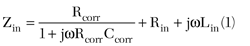
Setting ImZin = 0, Lin is given by:

The real part of the input impedance ReZin can be rewritten as
This means that, by proper selection of the parameters of the correction circuit elements Rcorr and Ccorr, the real part of the input impedance ReZin can be increased to a desired level. For example, for Lin = 1.4 nH and Rin = 5 Ω, the resistance ReZin becomes equal to 50 Ω when Rcorr = 10 Ω and Ccorr = 3.1 pF.
According to the datasheet for a 5 W Nitronex GaN HEMT device NPTB00004, its input circuit can be equivalently represented by a series RLC circuit, as shown. Here, the input impedance becomes real and equal to 5 Ω at an operating frequency of approximately 1.85 GHz.6 The equivalent input series inductance Lin and capacitance Cin can be determined from two equations: ImZin = -23.8 Ω at 900 MHz and ImZin = 21.0 Ω at 3.5 GHz. The quality factor of the input circuit at the bandwidth frequency center, ƒ0 = 2.2 GHz, is Qin = ω0Lin/Rin = 3.87, which means that the achievable frequency bandwidth at the -3 dB power level can be approximately estimated as Δƒ = ƒ0/Qin = 568.5 MHz.
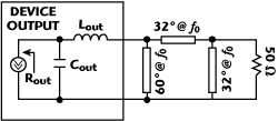
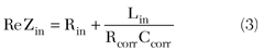
Figure 2 Output matching circuit equivalent representation.
In addition, it is necessary to take into account that the effect of the parasitic input resistance will increase at higher frequencies, resulting in a lower real part of the device transfer admittance Y21 = gm/(1 + jωRinCin), where gm is the device transconductance. Therefore, an additional LC matching circuit with optimized parameters can be added to the device input, which helps to improve the input broadband matching since the real part of the device input impedance is sufficiently small. Also, to compensate for excessive capacitive input reactance, a lossy shunt RL circuit with a transmission line having a quarter wavelength at the high bandwidth frequency ƒhigh is often used in broadband microwave power amplifiers, which further improves the input return loss.7,8

Figure 3 Small-signal frequency response of the load network.
Figure 2 shows the equivalent representation of the power amplifier load network, where the device output contains the parasitic shunt capacitance Cout and series inductance Lout, the negative effect of which on the frequency response shown in Figure 3 must be eliminated over an entire operating frequency range. The values of Cout and Lout can be evaluated similarly using the measured output device impedances at the same two boundary frequencies. The load resistance RL, which should terminate the device output to deliver a fundamental frequency output power Pout = 4 W or 36 dBm to the load, can be estimated based on a conventional Class B mode as:
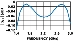
Figure 4 Optimized small frequency response of the load network.
which results in a value of 50 Ω for Vdd = 20 V. As a result, the output load network can represent a mixed lumped-distributed low pass π-type circuit with an inductive short series transmission line and a capacitive open-circuit stub. An additional short-circuited transmission line is necessary to supply DC power to the device. Figure 4 shows the optimized small-signal frequency response of the entire load network over a very wide frequency range. In this case, an efficiency improvement can be achieved by using a Class E load network with reactance compensation technique when a short-circuited transmission line together with the device output reactance provides the required inductive impedance at the fundamental frequency and capacitive reactances at the second and high-order harmonics.4
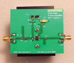
Figure 5 Test board of broadband GaN HEMT power amplifier.
Implementation and Test
The broadband transmission-line hybrid GaN HEMT power amplifier was fabricated on a 30 mil thick RO4350 substrate. Figure 5 shows the test board of this power amplifier using a 5 W Nitronex GaN HEMT RF power transistor NPTB00004. The broadband input matching circuit, output load network, and gate and drain bias circuits (having bypass capacitors at their ends) are fully based on the 50 Ω microstrip lines of different optimized electrical lengths according to the theoretical predictions and computer optimization using ADS simulation.
Figure 6 shows the test results with an output power of 36 ± 0.5 dBm and a drain efficiency of 57 ± 3 percent over most part of the operating frequency range from 1.7 to 2.7 GHz (with a gate bias voltage Vg = -1.3 V, a quiescent current Iq = 50 mA and a drain supply voltage Vdd = 20 V), achieved without any tuning of the broadband input matching circuit and load network. In this case, a power gain of approximately 13 dB and an input return loss better than 6.5 dB were measured, as shown in Figure 7. It should be noted that, according to the load-pull data for a 5 W Nitronex GaN HEMT device NPTB00004, its typical drain efficiency of approximately 55 percent can only be achieved at 2.5 GHz.6
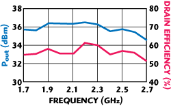
Figure 6 Output power and drain efficiency of the amplifier.

Figure 7 Power gain and input return loss of the amplifier.
Conclusion
A low-cost and efficient solution for a broadband transmission-line GaN HEMT power amplifier, based on a 5 W Nitronex NPTB00004 device in a plastic package, is analyzed and described. This power amplifier can be used in various wireless applications covering simultaneously different communication standards such as DCS1800, PCS1900, CDMA2000, W-CDMA or LTE. The theoretical analysis is based on a simple analytical estimation of the parameters of the input lossy matching circuit and nominal output resistance with further computer optimization of the circuit parameters of the entire power amplifier schematic. The test board with the implemented broadband transmission-line GaN HEMT power amplifier was measured and a drain efficiency over 52 percent and a flat output power of approximately 36 dBm at a low supply voltage of 20 V have been achieved across the wide range of operating frequencies from 1.7 to 2.7 GHz.
References
- Y.F. Wu, R.A. York, S. Keller, B.P. Keller and U.K. Mishra, "3 to 9 GHz GaN-based Microwave Power Amplifiers with L-C-R Broadband Matching," IEEE Microwave and Guided Wave Letters, Vol. 9, No. 8, August 1999, pp. 314-316.
- K. Krishnamurthy, D. Green, R. Vetury, M. Poulton and J. Martin, "0.5 to 2.5, 10 W MMIC Power Amplifier in GaN HEMT Technology," 2009 IEEE Compound Semiconductor Integrated Circuits Symposium Digest.
- H. Xu, S. Gao, S. Heikman, S.I. Long, U.K. Mishra and R.A. York, "A High-efficiency Class E GaN HEMT Power Amplifier at 1.9 GHz," IEEE Microwave and Wireless Components Letters, Vol. 16, No. 1, January 2006, pp. 22-24.
- A. Grebennikov and N.O. Sokal, Switchmode RF Power Amplifiers, Newnes, Elsevier, Maryland Heights, MO, 2007.
- M.P. van der Heijden, M. Acar and J.S. Vromans, "A Compact 12 W High-efficiency 2.1 to 2.7 GHz Class E GaN HEMT Power Amplifier for Base Stations," 2009 IEEE MTT-S International Microwave Symposium Digest, pp. 657-660.
- Nitronex Corp., NPTB00004 Datasheet, NDS-002 Rev. 2, September 2008.
- K.B. Niclas, "On Design and Performance of Lossy Match GaAs MESFET Amplifier," IEEE Transactions on Microwave Theory and Techniques, Vol. 30, No. 11, November 1982, pp. 1900-1906.
- Y. Ito, M. Nii, Y. Kohno, M. Mochizuki and T. Tagaki, "A 4 to 25 GHz 0.5 W Monolithic Lossy Match Amplifier," 1994 IEEE MTT-S International Microwave Symposium Digest, pp. 257-260.
Andrei Grebennikov received his Dipl. Ing. degree in radio electronics from the Moscow Institute of Physics and Technology and his PhD degree in radio engineering from the Moscow Technical University of Communications and Informatics in 1980 and 1991, respectively. He obtained long-term academic and industrial experience working with the Moscow Technical University of Communications and Informatics (Russia), the Institute of Microelectronics (Singapore), M/A-COM (Ireland), Infineon Technologies (Germany/Austria) and Bell Laboratories (Ireland) as an engineer, researcher, lecturer and educator.