
Since the Federal Communications Commission's (FCC) release of the frequency band from 3.1 to 10.6 GHz for commercial purposes,1 the UWB radio system has been receiving great attention from both academy and industry. As an essential component, UWB bandpass filters, with good performance, compact size and easily-implemented structures, are in high demand. So far, several prototypes of UWB filters have been reported.
Ishida and Araki have reported a microstrip ring filter with dual stopbands, below 3.1 GHz and above 10.6 GHz, which was the first UWB filter.2 However, this filter has many problematic issues, such as unexpected passbands below 3.1 GHz, narrow stopbands, large size and complex configuration.
Due to their geometric simplicity, parallel coupled microstrip lines were commonly used to design bandpass filters. Generally, this procedure is used for bandwidths less than approximately 20 percent.3 To overcome this limitation, a three-coupled-line microstrip structure was proposed4 to design a bandpass filter with a fractional bandwidth of 50 percent. However, the greater the fractional bandwidth, the smaller the gap size is required to enhance the coupling. For UWB filter design, the necessary gap size is still too narrow to be fabricated. Furthermore, ground plane aperture compensation techniques were successfully used for significant increasing of coupling coefficient between parallel coupled lines, thus leading to wider bandwidths.5,6
Stepped-impedance resonators (SIR) have demonstrated their advantageous efficiency for UWB bandpass filters. A UWB bandpass filter with five transmission poles has been proposed,7 using a multiple-mode resonator (MMR). By properly allocating the first three resonance peaks quasi-equally within the UWB band, a short-circuited coplanar waveguide (CPW) MMR bandpass filter was realized.8
A two-stage UWB bandpass filter, using a capacitive-ended interdigital coupled-line topology, was adopted to achieve improved out-of-band performance.9 Note that some of these filters7,9 lack design method and synthesis procedure. Later, a modified stub-loaded multiple-mode resonator was proposed,10-13 aiming to allocate the first resonant frequencies within the 3.1 to 10.6 GHz band while suppressing spurious harmonics at the upper-stopband. A quasi-Chebyshev bandpass filter with nine transmission poles was synthesized using three triple-mode SIRs (two-layer broadside-coupled structure).14 Ground plane aperture techniques, increasing coupling between pairs MMR resonators, were also widely investigated to improve the out-band rejection in UWB filters.14,15
Stub bandpass filters with several configurations could also be used to meet UWB mask requirements.16-19 Connecting lines between short-circuited stubs were meandered in order to reduce the filter size.16,17 These UWB filters have sharp rejection, but their spurious response would degrade the out-of-band response and an increase in the number of sections may lead to large insertion loss, as well as poor group delay. In addition, stepped impedance open stubs were implemented on this kind of structure to realize transmission zeros and get sharper attenuations.18,19 Tight coupling in a microstrip to CPW or slotline transition has also been investigated.20-24 The use of microstrip-to-CPW transition has received great attention providing a wide bandpass operation with a good trade-off in terms of insertion loss and group delay flatness.20 A UWB filter with a multiple-mode resonator was proposed using the microstrip-to-CPW transitions as inverter circuits.21 Composite transition lines exhibiting cross-coupling and slow-wave behavior were later proposed,22 leading to more compact devices. Recently, back-to-back microstrip-slotline cross-junction transition was rearranged to make up a novel class of UWB bandpass filter with lenient tolerance in fabrication.23,24
Basically, a wide bandwidth filter may be implemented by a direct cascade of the low-pass and high-pass filters. Wideband coplanar-waveguide bandpass filters based on the cascade of CPW low- and high-pass periodic structures were constructed.25 To save circuit area, a high-pass filter, realized by shunt quarter-wave short-circuited stubs, was embedded with a stepped-impedance low-pass filter.26 As a result of the use of a low degree high-pass filter, the filter lacked selectivity or sharpness at the lower frequency. Note that a suspended stripline technology combining low loss with reduced size was also used to fabricate this composite filter.27 Analytical techniques to synthesize an isolated cascade of high- and low-pass sections based on an iterative algorithm for both Butterworth and Chebychev cases were also reported.27 In a previous work,28 several UWB filters were realized in a semi-lumped approach, using both surface-mounted (SMT) capacitors and microstrip transmission lines. Thanks to the slow-wave behavior introduced by capacitively loaded transmission lines, a high degree of miniaturization was demonstrated.29 In this article, a technique of spurious suppression is studied.
Principle
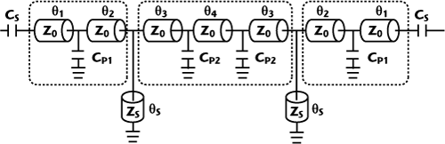
Figure 1 Equivalent circuit of the proposed semi-lumped UWB filter.
Configuration and Synthesis Technique
Figure 1 shows the equivalent electrical circuit of the proposed semi-lumped UWB bandpass filter. Following the same principle as Hsu, et al.,26 low-pass and high-pass filters are combined. The high-pass filter is realized by shunt quarter-wave short-circuited stubs. The stepped impedance low-pass filter that was used is replaced in this work by a low-pass filter based on capacitively loaded transmission lines as published previously.29 Compared to the distributed filter,26 a size reduction reaching 85 percent was demonstrated, thanks to the use of the semi-lumped technology.28 In addition, two series capacitors are added at the near- and far-ends of the filter in order to give a sharper rejection around the lower stopband.
In order to investigate the synthesis procedure, a UWB filter centered at 0.77 GHz with a 142 percent relative 3 dB bandwidth is considered. In this article, the center frequency ƒc of the bandpass filter is given by:

where ƒL and ƒH are the low and high 3 dB cut-off frequencies, respectively.
The proposed synthesis procedure concerns the establishment of a rough initial estimation of the filter's parameters, by setting both low and high cut-off frequencies. To simplify the study, an initial design with ideal transmission lines and capacitors is adopted. In addition, identical series transmission lines' electrical lengths are first considered, that is θ = θ1 = θ2 = θ3 = θ4. The main advantage of this filter topology is the independent control of both low and high cut-off frequencies. The upper and lower cut-off frequencies are respectively controlled by the low-pass and high-pass sections.
The low-pass sections are realized by capacitively loaded transmission lines following the same principle of the low-pass filters published previously.29 In this previous work, the low-pass section was studied and the design equations relating the characteristic impedance Z0, the loading capacitance Cp and the transmission line electrical length θ to the cut-off frequency ƒH were derived. For a characteristic impedance equal to 120 Ω and assuming a 1.5 GHz high cut-off frequency, the equations established lead to Cp= 3.1 pF and θ = 29° at 1.5 GHz.
While the high cut-off frequency ƒH is adjusted by the low-pass section, the low cut-off frequency ƒL is directly controlled by the short-circuited stubs electrical length θs. A simple tuning carried out with Agilent ADS30 revealed that the electrical length θs should be set to 23° at 0.4 GHz.
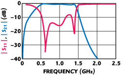
Figure 2 Simulated response of the UWB bandpass filter.
Currently, rough initial values for Cp, θ and θs are available. The filter response simulated using the following parameters—Cp= 3.1 pF, θ 29° at 1.5 GHz, θs = 23° at 0.4 GHz—is illustrated in Figure 2. As a result, the cut-off frequencies obtained are 0.4 and 1.45 GHz, respectively. The simple design method described above is sufficient for a rough estimate of the filter's parameters. Note that the simulated filter suffers also from a poor matching in the passband, with a return loss reaching only 8†dB at approximately 1.3 GHz. However, the return loss will be improved in the second step of the design when the filter will be optimized.
For the second step consisting of a whole optimization of the complete filter, a microstrip technology is considered. A Rogers™ RO4003 substrate with relative permittivity εr = 3.38, substrate thickness h = 813 μm and dielectric losses tan = 0.0027 has been adopted. Also, the T junctions, surface-mounted capacitors, soldering pads and via holes models are taken into account. Complete models taking into account the parasitic series elements with an inductance of 0.35 nH and a resistance of 0.25 Ω are considered to get more accurate simulation responses. In order to maximize the degrees of freedom and improve filter performance, the series transmission lines' electrical length and the capacitors' value are not considered as equal anymore.


Figure 3 Simulated response of the proposed UWB semi-lumped bandpass filter.
The UWB filter is optimized using Agilent ADS.30 The transmission line's characteristic impedance has been set to 120 Ω, leading to a strip width W equal to 250 μm. The value for the series capacitors added in the near- and far-end of the UWB bandpass filter to improve the low stop-band rejection is fixed at 6.8 pF, leading to a small impedance compared to 50 Ω, keeping unchanged the low cut-off frequency. Table 1 lists the electrical lengths and capacitor's values obtained after optimization for the UWB filter. Figure 3 gives the simulation results to 8 GHz, using the parameters' values given in Table 1. As illustrated, the return loss is better than 20 dB in the whole passband; the insertion loss is limited to 0.2 dB at the center frequency. The shape factor, defined between -3 and -20 dB, equals 1.3:1. In the simulated response, a spurious frequency occurs at approximately 5 GHz, leading to an out-of-band rejection level of -40 dB to only 4.5 GHz, that is 4.5 times the center frequency. The study of the spurious origin is carried out in the next section where a simple original technique to reject theses spurious frequencies is suggested.

Figure 4 Transmission Zeros of the UWB bandpass filter up to 8 GHz.
Spurious Analysis and Improvement
The basic principle of spurious suppression is based on the transmission zeros repartition in the frequency response. As illustrated in Figure 4, three transmission zeros are observed respectively at 2.2, 3.2 and 6 GHz. A possible solution to reject the spurious frequencies and improve the rejection band width could be to move the transmission zeros, either to push the 3.2 GHz transmission zero to higher frequencies, or to pull the 6 GHz transmission zero to lower frequencies. Therefore, the study of the origin of these transmission zeros has to be carried out first.
Transmission zeros located at 2.2 and 3.2 GHz are due to the resonance of the LC shunt circuit formed by the SMT capacitor and the parasitic inductances. This parasitic inductance is the sum of the intrinsic SMT capacitor, the soldering pads and the via holes inductances. Considering the capacitor's model and the via hole's dimensions, its value Ls can be estimated to be 1.3 nH. The transmission zero location is then easily calculated using the expression of the LC resonant frequency:

Indeed, the 2.2 GHz transmission zero is introduced by the resonant circuit formed by the 3.9 pF capacitor and the series parasitic inductance Ls = 1.3 nH, while the 3.2 GHz transmission zero is related to the 1.8 pF capacitor. As the high cut-off frequency is controlled by the LC circuit, the lower transmission zeros could not be moved. A modification of these transmission zeros will affect the passband response of the UWB filter.

Figure 5 UWB filter equivalent circuit with capacitively loaded stubs.
The transmission zero appearing at 6 GHz is due to the short-circuited stub resonance that presents a 180° electrical length near 6 GHz. A solution for spurious suppression would be to pull this transmission zero to lower frequencies. This could be easily achieved by increasing the stub electrical length. However, as the low cut-off frequency is fixed by the stub's length, the low frequency electrical length should not be modified. Thus, capacitively loaded stubs could be successfully used for spurious suppression, leading to the whole UWB bandpass filter equivalent electrical circuit given in Figure 5. A capacitively loaded stub will behave as an unloaded stub at low frequency because the capacitor's susceptance is high, so that the stub's behavior remains unchanged. When the frequency increases, the loading capacitor becomes significant compared to the stub's transmission line distributed capacitor, and the wave velocity in the loaded stub will decrease, leading to a lower resonant frequency for the stub.
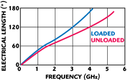
Figure 6 Comparison of the electrical length of the capacitively loaded and unloaded stubs.
Using Agilent ADS,30 the UWB filter with capacitively loaded stubs has been optimized. The electrical lengths (θs1 and θs2) and the stub's loading capacitor Csp optimized values have been set to 5° and 11° and 0.4 pF, respectively. The equivalent electrical length of both loaded (θ's) and unloaded (θs) stubs are plotted in Figure 6. While the unloaded stub electrical length increases proportionally versus frequency, the loaded stub electrical length increases quickly with frequency, leading to a lower resonant frequency of 4.2 GHz. Thus, the transmission zero will be shifted to lower frequencies. In the lower band, the electrical length for both loaded and unloaded stubs are quite similar. The filter passband remains quite unchanged with the capacitively loaded stubs configuration.

Figure 7 Simulated insertion loss of the UWB filter with loaded and unloaded stubs.
Figure 7 compares the UWB filter insertion loss with both loaded and unloaded stubs. Whereas the filter response remains unchanged in the passband, the loading capacitor effect appears for higher frequencies. When the capacitively loaded stubs are used, the third transmission zero that was located at 6 GHz occurs now at 3.8 GHz, while the first two transmission zeros due to LC resonance remain fixed. Consequently, the high frequency rejection band, defined below an attenuation of -40 dB, is enlarged to about 6.5 GHz, that is more than eight times the filter's center frequency of 0.77 GHz.
UWB Filters Realization and Measurements
In this section, several UWB filters with 3 dB bandwidth of 142 percent centered at 0.77 GHz are realized and measured. The photograph of the realized filters is shown in Figure 8. Filters with loaded and unloaded stubs have been fabricated. For filters with loaded stubs, SMT and patch capacitors are considered. SMT capacitors with a 0402 case (0.5 mm by 1 mm) have been used. All the realized filters are 3.7 cm in length.

Figure 8 Photograph of the fabricated filters: (a) unloaded stubs, (b) stubs loaded with SMT capacitors and (c) stubs loaded with patched capacitors.
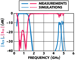
Figure 9 Simulated and measured results for the UWB filter with unloaded stubs.
First, measured and simulated results of the UWB filter with unloaded stubs are given in Figure 9. A good agreement is observed in the filter passband. A wideband of 1.1 GHz is achieved leading to the expected bandwidth of 142 percent. The measured return and insertion loss are found to be higher than 18 dB and lower than 0.3 dB over the passband, respectively. The first spurious response appears around 4.5 GHz. A slight shift of about 400 MHz is observed between simulations and measurements. This shift is probably due to the capacitor's model that is not sufficiently accurate at high frequencies. The measured rejection band, if a minimum of 40 dB attenuation is considered, extends to approximately 4.2 GHz, that is 5.4 times the center frequency.
Measurements of both filters with unloaded and loaded with SMT capacitors stubs are compared in Figure 10. While the bandwidth is quite the same for the two topologies, the return loss is improved to 20 dB with the capacitively loaded stubs. With the introduction of SMT capacitors, the first spurious peak is shifted from approximately 4.5 to 6.7 GHz. The measured rejection band (a minimum 40 dB attenuation is still considered) extends to approximately 6 GHz when capacitively stubs are used, that is more than eight times the center frequency, showing a significant improvement.
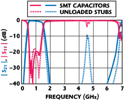
Figure 10 Measured frequency responses for UWB filters with unloaded and loaded with SMT capacitor stubs.
Next, Figure 11 shows the comparison between the measurement results to 8 GHz, for filters with stubs loaded by SMT and patch capacitors. With patch capacitors, the return loss is better than 18†dB in the passband and the rejection band is slightly enlarged from 6 to 6.6†GHz. It can be concluded that capacitively loaded stubs can be successfully used for spurious suppression.
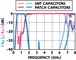
Figure 11 Measured frequency responses for UWB filters with capacitively loaded stubs.
For miniaturization purposes, bended stubs could be used. This technique could not be easily achieved with stubs loaded by patch capacitors. Therefore, a filter with bended stubs loaded by SMT capacitors was fabricated. Figure 12 shows a photograph of the miniaturized filter. The miniaturization improvement with bended stubs reaches 55 percent (in terms of surface area) compared to the filter with straight stubs. A good agreement between measurement and simulation results is observed. The return loss is better than 22 dB and the rejection band extends to approximately 6 GHz.

Figure 12 Simulated and measured response for the UWB filter with bended capacitively loaded stubs.
Conclusion
In this article, a new topology of semi-lumped UWB bandpass filter has been proposed. It is based on the combination of low-pass and high-pass filters. The synthesis method of the bandpass filter has been developed and validated by simulations. Filters centered at 0.77 GHz with a relative bandwidth of 142 percent have been designed and fabricated. Simulated and measured results have shown a good agreement in terms of return loss (better than 18 dB) and insertion loss (lower than 0.3 dB). A spurious suppression technique, using capacitively loaded stubs, has been carried out and has demonstrated its efficiency to eliminate spurious responses up to more than eight times the center frequency. A miniaturization better than 55 percent has also been achieved by a simple stub bending.
References
- FCC, "Revision of Part 15 of the Commission's Rules Regarding Ultra-Wideband Transmission System," Technical Report ET-Docket 98-153, 14 February 2002.
- H. Ishika and K. Araki, "A Design of Tunable UWB Filters," 2004 International Workshop on Ultra Wideband Systems Digest, Kyoto, Japan, pp. 424-428.
- K.S. Chin, L.Y. Lin and J.T. Kuo, "New Formulas for Synthesizing Microstrip Bandpass Filters with Relatively Wide Bandwidths," IEEE Microwave and Wireless Components Letters, Vol. 14, No. 5, May 2004, pp. 231-233.
- J.T. Kuo and E. Shih, "Wideband Bandpass Filter Design with Three-line Microstrip Structures," 2001 IEEE MTT-S International Microwave Symposium Digest, pp. 1593-1593.
- Y.A. Kolmakov and I.B. Vendik, "Compact Ultra-wideband Bandpass Filter with Defected Ground Plane," 2005 European Microwave Conference Digest, pp. 21-24.
- M.K. Mandal and S. Sayal, "Compact Wideband Bandpass Filter," IEEE Microwave and Wireless Components Letters, Vol. 16, No. 1, January 2006, pp. 46-48.
- L. Zhu, S. Sun and W. Menzel, "Ultra-wideband (UWB) Bandpass Filters Using Multiple-mode Resonator," IEEE Microwave and Wireless Components Letters, Vol. 16, No. 11, November 2005, pp. 796-799.
- J. Gao, L. Zhu, W. Menzel and F. BöGelsack, "Short-circuited CPW Multiple-mode Resonator for Ultra-wideband (UWB) Bandpass Filter," IEEE Microwave and Wireless Components Letters, Vol. 16, No. 3, March 2006, pp. 104-107.
- S. Sun and L. Zhu, "Capacitive-ended Interdigital Coupled Lines for UWB Bandpass Filters with Improved Out-of-band Performances," IEEE Microwave and Wireless Components Letters, Vol. 16, No. 8, August 2006, pp. 440-443.
- S.T. Li and Q.X. Chu, "A Compact UWB Bandpass Filter with Improved Upper-stopband Performance," 2008 International Conference on Microwave and Millimeter Wave Technology Digest, pp. 363-365.
- S.W. Wong and L. Zhu, "Ultra-wideband (UWB) Microstrip Bandpass Filters with Improved Upper-stopband and Miniaturized Size," 2007 Asia-Pacific Microwave Conference Digest.
- S.W. Wong and L. Zhu, "EBG-embedded Multiple-mode Resonator for UWB Bandpass Filter with Improved Upper-stopband Performance," IEEE Microwave and Wireless Components Letters, Vol. 17, No. 6, June 2007, pp. 421-424.
- R. Li and L. Zhu, "Compact UWB Bandpass Filter Using Stub-loaded Multiple-mode Resonator," IEEE Microwave and Wireless Components Letters, Vol. 17, No. 1, January 2007, pp. 40-43.
- J.T. Kuo, Y.C. Chiou and E. Cheng, "High Selectivity Ultra-wideband (UWB) Multimode Stepped-impedance Resonators (SIR) Bandpass Filter with Two-layer Broadside-coupled Structure," 2007 Asia-Pacific Microwave Conference.
- H. Wang and L. Zhu, "Aperture-backed Microstrip Line Multiple-mode Resonator for Design of a Novel UWB Bandpass Filter," 2005 Asia-Pacific Microwave Conference.
- W.T. Wong, Y.S. Lin, C.H. Wang and C.H. Chen, "Highly Selective Microstrip Bandpass Filters for Ultra-wideband (UWB) Applications," 2005 Asia-Pacific Microwave Conference.
- H. Shamman and J.S. Hong, "A Novel Ultra-wideband (UWB) Bandpass Filter (BPF) with Pairs of Transmission Zeroes," Microwave and Wireless Components Letters, Vol. 17, No. 2, February 2007, pp. 121-123.
- P. Cai, Z. MA, X. Guan, X. Yang, Y. Kobayashi, T. Anada and G. Hagiwara, "A Compact UWB Bandpass Filter Using Two-section Open-circuited Stubs to Realize Transmission Zeros," 2005 Asia-Pacific Microwave Conference.
- X. Gong, J. Wang and W. Wang, "An Improved Design Method for UWB Filter Using Two-section Open-circuited Stubs," 2007 International Conference on Microwave and Millimeter Wave Technology Proceedings.
- K. Li, D. Kurita and T. Matsui, "An Ultra-wideband Bandpass Filter Using Broadside-coupled Microstrip-coplanar Waveguide Structure," 2005 IEEE MTT-S International Microwave Symposium Digest, pp. 675-678.
- H. Wang, L. Zhu and W. Menzel, "Ultra-wideband Bandpass Filters with Hybrid Microstrip/CPW Structure," IEEE Microwave and Wireless Components Letters, Vol. 15, No. 12, December 2005, pp. 844-846.
- T.N. Kuo, S.C. Lin and C.H. Chen, "Compact Ultra-wideband Filters Using Composite Microstrip-coplanar-waveguide Structure," IEEE Transactions on Microwave Theory and Techniques, Vol. 54, No. 10, October 2006, pp. 3772-3778.
- R. Li and L. Zhu, "Ultra-wideband (UWB) Bandpass Filters with Hybrid Microstrip/slotline Structures," IEEE Microwave Wireless Components Letters, Vol. 17, No. 11, November 2007, pp. 778-781.
- R. Li and L. Zhu, "Compact UWB Bandpass Filter on Hybrid Microstrip/Slotline Structure with Improved Out-of-band Performances," 2008 International Conference on Microwave and Millimeter Wave Technology.
- Y.S. Lin, W.C. Ku, C.H. Wang and C.H. Chen, "Wideband Coplanar-waveguide Bandpass Filters with Good Stopband Rejection," IEEE Microwave Wireless Components Letters, Vol. 14, No. 9, September 2004, pp. 422-424.
- C.L. Hsu, F.C. Hsu and J.T. Kuo, "Microstrip Bandpass Filter for Ultra-wideband (UWB) Wireless Communications," 2005 IEEE MTT-S International Microwave Symposium Digest, pp. 679-682.
- W. Menzel, M. Tito and L. Zhu, "Low-loss Ultra-wideband (UWB) Filters Using Suspended Stripline," 2005 Asia-Pacific Microwave Conference, December 2005.
- D. Kaddour, J.D. Arnould and P. Ferrari, "A Semi-lumped Microstrip UWB Bandpass Filter," International Journal of Microwave and Wireless Technologies, Vol. 1, No. 1, February 2009, pp. 57-64.
- D. Kaddour, E. Pistono, J.M. Duchamp, J.D. Arnould, H. Eusebe, P. Ferrari and R.G. Harrison, "A Compact and Selective Low-pass Filter with Reduced Spurious Responses Based on CPW Tapered Periodic Structures," IEEE Transactions on Microwave Theory and Techniques, Vol. 54, No. 6, June 2006, pp. 2367-2375.
- ADS, Agilent Technologies Inc., Palo Alto, CA.