
The direct plated copper (DPC) process on metallized ceramic substrate was originally created to replace the direct bonded copper (DBC) process because of its better electrical, thermal and mechanical performance.1 Compared to DBC, DPC provides a very strong bond strength between the Al2O3/AlN substrate and the copper metal, due to the use of a thin film bonding layer.2 DPC also has a good ability in thickness control for the copper layer, from very thin to very thick. For fine pitch design, a minimum conductor line width/spacing of 3 mils can be easily obtained, and via holes are filled with copper for good electrical and thermal characteristics. By using the proposed DPC substrate, superior performance can be obtained compared to other technologies in terms of its features and applications, which includes high circuit density, outstanding high-frequency characteristics, excellent thermal management and heat-transfer performance, outstanding solderability, and wire-bonding assembly characteristics. These DPC substrates can therefore be widely used for high frequency components that require high power and high heat.3
In this article, the DPC fabrication is briefly described with a process flow chart, to introduce several key attributes of this process. A simple electrical characterization for DPC substrate is then utilized to extract the high-frequency dielectric constant and dissipation factor. Finally, a 10 GHz, parallel-coupled line bandpass filter is designed to validate the extracted dielectric parameters and the excellent high-frequency performance of a DPC metallized substrate.
Direct Plated Copper Process
The entire DPC process basically comprises the steps displayed in Figure 1, which include defining holes in the ceramic substrate, sputtering a copper film onto the ceramic substrate, forming a dry film onto the copper film, forming a circuit diagram with exposure and development, plating copper leads, removing the dry film and etching the seed metal copper.3 The detailed processes have been described by S.P. Ru,4 with more theoretical explanations and drawings.

Figure 1 DPC process flow chart.
With the flow chart shown, the DPC process is started by defining holes on the bare ceramic substrate with a laser. These holes can be used as via holes to communicate between both sides of the ceramic substrate if it is necessary for some specific designed layout. Then a copper film, used as a seed metal layer, is sputtered on the opposite sides of the ceramic substrate so that it is covered with a copper layer. From the artwork describing the circuit diagram, a photomask is made using conventional photomask technology. The photomask is flatly positioned and adheres to the dry film on the ceramic substrate, which is sent into an exposing chamber.
After creating a vacuum in the exposing chamber, ultraviolet rays irradiate the dry film through the photomask, which is polymerized by the ultraviolet radiation. The dry film, which is not irradiated by the ultraviolet rays, does not react and keeps its chemical composition. The development process etches the polymerized part of the dry film by chemical cleaning or physical cleaning. In this way, some parts of the copper film are exposed from the dry film; those parts of the copper film will form the required circuit diagram as per the artwork of the circuit, in order to produce the required copper areas of a circuit on the ceramic substrate. Thus, the circuit layout can be printed on the dry film.
Copper is then deposited to fill the exposed parts of the dry film on the ceramic substrate, with suitable conductor thickness and width, by a plating technology to form the copper circuit. By the above processes, the metallized circuit area has slender, flat and smooth characteristics, and the heat dissipation is good. Then nickel and gold are deposited on the upper surface of the copper. The nickel film prevents the atoms of the copper leads diffusing into the gold film. The gold film avoids the oxidization of the conductor surface and improves the adhesion for the gold bonding wires. An optical resistance is formed on the upper surface of the copper. The remaining dry film on the ceramic substrate is then removed. After stripping the dry film, the copper circuit is protected by the nickel and gold films. The detaching copper film process etches the copper film not protected by the optical resist.
Due to the processes described and the materials used, several key attributes of the DPC process can be summarized as below:
- Superior thermal performance
- Low electrical resistance conductor lines
- Stable up to temperature > 340°C
- Accurate feature location, compatible with automated, large format assembly
- Fine line resolution allowing high density of devices and circuitry
- Proven reliability
- Mechanically rugged ceramic construction
- Low cost, high performance ceramic solution
The applications of DPC metallized substrate can be selected on high-brightness LED (HBLED), substrates for solar concentrator cells, power semiconductor packaging and automotive motor control. In addition, DPC substrates with excellent electrical performance can be considered for RF/microwave components, which require very low loss.
Electrical Properties Extraction
In order to utilize DPC substrates for RF/microwave applications, the dielectric properties must be extracted. Dielectric characterization is a very important issue for electronic packaging designs since electrical behavior is greatly influenced by the dielectric constant and dielectric loss at high frequencies.

Figure 2 DPC microstrip parallel-coupled resonators with distinct output connections: (a) PCMR1 and (b) PCMR4.
There are numerous reported methods in the published literature.5-8 Many of these methods have one or several limitations, such as expensive and complicated instrumentation, difficult-to-fabricate fixtures, measured dielectric properties only valid for one particular frequency, poor repeatability, and inability to obtain both dielectric constant and dielectric loss. However, in this article, a simple approach is used to obtain the accurate dielectric factors for further substrate design and simulation.
Holzman used a computer model of the resonator to extract the dielectric data.9 Once the circuit is modeled accurately with a computer-aided design (CAD) simulator, the substrate's dielectric properties can be determined by comparing the predictions from the simulator with the measured characteristics. This empirical/analytical approach has been demonstrated by a number of researchers in the microwave field.

Figure 3 Measured and simulated results for the microstrip parallel-coupled resonators: (a) PCMR1 and (b) PCMR4.
Therefore, to extract high-frequency dielectric data for DPC substrate, two modified microstrip parallel-coupled resonators with distinct zeros over a broad bandwidth were fabricated. Figure 2 shows the photos of parallel-coupled microstrip resonators (PCMR). The PCMR1 shown affects transmission zeros with more depth at lower frequencies; PCMR4 generates transmission zeros with deeper depth at higher frequencies. The two resonators have the same coupled-line structure with a line distance of 570 mils and a spacing of 12 mils, but opposite output connections. From the measurements of the two PCMRs, these zeros are sufficient to interpolate correct dielectric values with good accuracy under a broadband frequency response. However, the first transmission zero for PCMR1 and PCMR4 are at 5.2 and 4.2 GHz, respectively, and repeating approximately at every resonant frequency over the band. To make a preliminary simulation of the resonators, a dielectric constant of 9.5 and a dielectric loss of 0.004 were assumed for DPC substrate in ADS Momentum simulation.
The testing setup consisted of an Agilent E8364A network analyzer, an Anritsu Universal Test Fixture with two K-connector coaxial input ports, and a ground-plane backed DPC metallized substrate with the microstrip resonators. In addition, a TRL calibration is adopted by using DPC fabricated calibration kits to calibrate at the same reference plane of the PCMRs. The comparisons between simulated and measured insertion losses for PCMR1 and PCMR4 are shown in Figure 3.

Figure 4 Measured and simulated results for the microstrip parallel-coupled resonator.
From the measurements, it is obvious that the assumed dielectric values are in error, with the error increasing at higher frequencies. To extract the correct dielectric constant and dielectric loss, these values are adjusted in ADS Momentum to match the frequency response until the predicted zero matches the measured zero. Figure 4 shows the fitted results for two PCMRs up to 14 GHz, after adjusting the dielectric parameters. In this case, the rise in these two parameters of DPC substrate is from 9.5 to 9.75 for the dielectric constant and 0.0004 to 0.002 for the dielectric loss, respectively. These values are more accurate than the assumed data at higher frequencies and can be widely used for substrate design and simulation.

Figure 5 Photograph of the 10 GHz parallel-coupled line filter using DPC technology.
MICROWAVE CIRCUIT DESIGN
To validate the accuracy of extracted dielectric data, a microwave filter fabricated on a DPC substrate was demonstrated. This BPF, using a parallel-coupled line structure, has a center frequency of 10 GHz, a bandwidth of 15 percent, 0.1 dB equal-ripple response and third-order topology, and is shown in Figure 5. The BPF was designed and optimized with ADS Momentum using the extracted dielectric constant and dielectric loss. The TRL calibration kits were also fabricated on DPC substrates to cover the frequency range from 4 to 14 GHz.
With these test standards, the Anritsu test fixture's coax-to-microstrip transitions and the microstrip lines up to the input and output ports of the filter can be de-embedded. The measured insertion loss and return loss are shown in Figure 6. Based on these experimental results, a good prediction of the filter response is achieved by using the extracted dielectric values in the EM simulator. The measured insertion loss of the BPF is only 0.5 dB at 10 GHz. It clearly demonstrated that the DPC process, fabricated with a ceramic substrate and copper conductor, provides excellent low-loss performance at high frequencies and offers the excellent ability to be used in RF packaging and microwave devices.
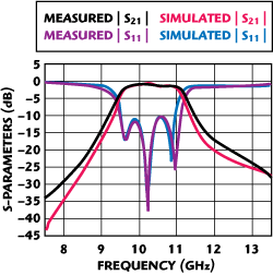
Figure 6 Measured and simulated characteristics of the 10 GHz DPC parallel-coupled line filter.
Conclusion
This article presents a DPC metallized substrate including the process flow, electrical properties extraction and a microwave circuit design. Owing to the use of the ceramic substrate and metallized copper conductor, the DPC substrate achieves good high-frequency electrical characteristics. Meanwhile, a simple extraction method to obtain the dielectric constant and dielectric loss for the DPC substrate was proposed, and a 10 GHz parallel-coupled line BPF with 0.5 dB insertion loss was built for further verification. This article clearly demonstrates that the DPC metallized substrate is quite suitable for RF and microwave package design, with its excellent low-loss performance.
References
- M. Entezarian and R.A.L. Drew, "Direct Bonding of Copper to Aluminum Nitride," Materials Science and Engineering, A-212, July 1996, pp. 206-212.
- J. Schulz-Harder, "Advantages and New Development of Direct Boded Copper Substrates," Microelectronics Reliability, Vol. 43, No. 3, 2003, pp. 359-365.
- "DPC-Direct Plated Copper Thin Film Technology," Tong Hsing, www.ready-sourcing.com/sourcing-news/electronic/dpc.html.
- S.P. Ru, "Method for Removing Voids in a Ceramic Substrate," US Patent, US 6,800,211 B2, October 2004.
- M.K. Das, S.M. Voda and D.M. Pozar, "Two Methods for the Measurement of Substrate Dielectric Constant," IEEE Transactions on Microwave Theory and Techniques, Vol. 35, No. 7, July 1987, pp. 636-642.
- S.H. Chang, H. Kuan, H.W. Wu, R.Y. Yang and M.H. Weng, "Determination of Microwave Dielectric Constant by Two Microstrip Line Method Combined with EM Simulation," Microwave and Optical Technology Letters, Vol. 48, No. 11, November 2006, pp. 2199-2121.
- H. Yue, K.L. Virga and J.L. Prince, "Dielectric Constant and Loss Tangent Measurement Using a Stripline Fixture," IEEE Transactions on Components, Packaging and Manufacturing Technology, Part B, Vol. 21, No. 4, November 1998, pp. 441-446.
- P.A. Bernard and J.M. Gautray, "Measurement of Dielectric Constant Using a Microstrip Ring Resonator," IEEE Transactions on Microwave Theory and Techniques, Vol. 39, No. 3, March 1991, pp. 592-595.
- E.L. Holzman, "Wideband Measurement of the Dielectric Constant of an FR4 Substrate Using a Parallel-coupled Microstrip Resonator," IEEE Transactions on Microwave Theory and Techniques, Vol. 54, No. 7, July 2006, pp. 3127-3130.
Chien-Cheng Wei received his MS and PhD degrees in electronic engineering from Chang Gung University, Taoyuan, Taiwan, ROC, in 2004 and 2008, respectively. During his graduate study, he was involved with RFIC design, ultra-wideband/millimeter-wave IC design, and RF CMOS device modeling. In September 2008, he joined the R&D department, Tong Hsing Electronic Industries, where he is involved with RF packaging, RF module assembling, high-frequency characterization for packaging materials and substrates.
Chin-Ta Fan received his MS degree in electronic engineering from Chung Yuan Christian University, Chung-Li, Taiwan, ROC, in 2003. His research interests include the characterization of metal oxide materials and applications for EGFET sensors. He joined the R&D department of Tong Hsing Electronic Industries in 2003, and is involved with SiP assembling, direct plated copper (DPC) metallized substrate development and gold-to-gold interconnect (GGI) process evaluation.
Ta-Hsiang Chiang, R&D Manager of Tong Hsing Electronic Industries, has served in the company for more than 25 years. He is the R&D leader in charge of RF packaging, MEMS packaging, hybrid circuit assembling, DPC substrate fabrication and any other new process development.
Ming-Kuen Chiu, Vice President of Tong Hsing Electronic Industries, has worked at Tong Hsing for more than 30 years. Since joining the company in 1976 as an engineer, he has taken over all works in engineering, equipment, sales, marketing and new process developments.
Shao-Pin Ru, Vice President of Tong Hsing Electronic Industries, has served in the company for more than 30 years. He started in 1976 as an engineer and has had assignments in engineering, operations, sales, marketing and new business development. He received his MBA degree from National Chiao Tung University in 1980 and graduated with a BS in electrical engineering from National Taiwan University in 1974.