
The increasing demand of the wireless communication service creates a demand for broadband networks and higher operating frequencies in the market place. As the operating frequency shifts higher, the generation of low drive level, fast start-up, low phase noise and stable reference signal sources with low cost become challenging due to the frequency limitations of crystal resonator and device circuitry.1-12
Many research works6-10 have exploited different circuit architectures of Colpitts-type circuits, which usually play a role in improving start-up time, drive level and negative resistance characteristics of the crystal resonator above the 500 MHz range. However, they exhibit inferior phase noise performance in comparison to commercially available surface acoustic wave (SAW) resonator-based reference frequency standards at 622 MHz and above in the gigahertz ranges.
Recent analysis indicates that, by decreasing the Miller capacitance of the transistor used for the conventional Colpitts-type crystal oscillator, a reasonably high negative resistance value can be achieved in a gigahertz frequency band.4,5 Reducing the Miller capacitance improves the negative resistance values at UHF/VHF ranges, but at the cost of poor jitter, thermal stability and phase noise performances. To meet the above challenge, most such effort is in the direction of employing a phase locked loop (PLL) using a crystal resonator. The drawback of this approach is spurious oscillations in the fundamental mode due to the multiplying mechanism by the PLL circuit. This is causing deterioration in jitter characteristics and introducing bit error in the communication systems.4
Therefore, designing a low phase noise high frequency VCXO as a reference frequency standard is challenging for a given cost, size, stability, phase noise and power consumption. In this work, a high frequency VCXO topology is reported that has the characteristic features of high negative resistance and low drive level, while maintaining the thermal stability and phase noise performances. The reported VCXO circuit is validated by modifying a conventional Colpitts oscillator with an active mode-coupling mechanism that optimizes the performance of crystal oscillators, even those with relative low Q resonators, for low phase noise and high frequency fundamental VCXO applications.

Figure 1 Typical quartz crystal: (a)electrode model, (b) lumped element model and (c) impedance characteristics.
Design Theory
An important application of the crystal resonator is in a VCXO, where the crystal resonator is typically incorporated in series with a tuning diode to vary the oscillation frequency. But these resonators suffer from multi-mode resonances and crosstalk due to the large value of the series resistance (Rs) and parasitic holder capacitances (C0) at UHF/VHF frequencies (see Figure 1).
Crystal Resonator
Quartz crystal is a piezo-electrical material in which mechanical deformations due to vibrations (compression/torsion/shear) cause potential differences across the distinct surfaces and vice versa. With two electrodes evaporated on the quartz crystal, an electrical model is obtained that typically exhibits a multi-mode resonances pattern. The figure shows the typical impedance characteristics of an electro-mechanical crystal resonator, which vibrates due to the piezo-electric effect and exhibits multi-mode resonances. As depicted, to the right of the fundamental response, the next major response is the third overtone, then the fifth overtone, and so on.11
Since the crystal does not produce harmonics, overtone responses are not the harmonics of the fundamental. To design a high performance crystal oscillator, the oscillator circuit topology determines the crystal configuration (fundamental, overtone, parallel and series). In other words, the oscillator circuit topology forces the crystal resonator into either the fundamental (lowest major resonant response), overtone (major responses other than fundamental), parallel (one of the inductive regions of the crystal's reactance curve as shown) or series (one of the resistive points on the crystal's reactance curve) operation.
As described, the motional parameters (Lx, Cx and Rx) govern the natural series resonance, whereas C0 is the parallel holder capacitor and Cv denotes the tuning diode capacitor required for pulling up the resonant frequency.
The series (fs) and parallel (fp) resonances are given by11
As illustrated, the electrode holder capacitance C0 supports the pole that implies a parallel resonance (fp) and can be viewed as a parallel resonant circuit with capacitive transformations. From Equations 1 and 2, the mode separation (fs - f0) can be expressed through the figure of merit M as11

From Equation 3, the figure of merit M describes the existence of series (fs) and parallel (fp) resonance modes. Therefore, due care must be taken for suppressing the unwanted resonance mode; otherwise, it leads to mode jumping. For stable oscillations, the series resonance frequency fs (wanted oscillation mode) is to be tuned by a series tuning diode Cv; the relative frequency shift can be expressed as
From Equation 4, the frequency drift can be optimized as a correction factor, but Cv is temperature sensitive and induces relative change ∂f in fresonance (pulled up resonance frequency) as

where kCv is the temperature coefficient that causes relative frequency fluctuations with temperature as a legitimate penalty to pull up the overall frequency shifted due to holder capacitance C0 and package parasitics, although the overall performance degrades at higher UHF/VHF ranges.
However, if the condition for resonance at UHF/VHF frequency could be established at the fundamental, the crystal resonator oscillator could be designed with excellent jitter characteristics, without being influenced by the spurious characteristics from fundamental operation.4
Start-up and Drive-level Characteristics
Quartz crystal oscillators seem to have reached their limit in terms of the frequency stability. However, they are still attractive as a reference frequency standard for their volume, size, cost and relative low power consumption in steady state, especially for space communications. As the size of the communications equipment and portable electronics become smaller, the crystal resonator size also shrinks to meet the real estate constraints. The reduction in crystal resonator size demands for larger activation current in the resonator network.

Figure 2 Typical Colpitts oscillator circuit including noise contribution.

Figure 3 Typical Colpitts oscillator: (a) conventional and b) modified topology.
In the past, a crystal oscillator with automatic gain control (AGC) has been used as a low drive-level VCXO. A typical VCXO with AGC consists of the oscillator stage, amplifier stage and the rectifier stage. The output of the rectifier stage is fed back into the bias circuit to obtain steady-state oscillation at low drive level. Due to the large filter time constant in the rectifier stage, the start-up characteristic is very slow; therefore, an AGC approach is not suited for portable telephone sets, where frequent switch-on and switch-off of the power supply are repeated for the power saving of the batteries. In addition, it is difficult to maintain a low resonator drive-level current IR without reduction in the magnitude of the negative resistance Rn(t) of the conventional Colpitts-type circuit (see Figure 2).
The negative resistance and resonator drive level at steady state can be described for circuits shown as11

I1(x) and I2(x) are the modified Bessel functions of order 0 and 1, respectively. From Equations 6 and 7, the resonator current drive-level IR can be lowered by increasing the value of the feedback capacitor C2 for a given emitter current IE, but at the cost of reduction in the value of negative resistance Rn. In order to maintain the same value of negative resistance Rn as required to compensate the loss resistance of the resonator at steady-state oscillation, the value of feedback capacitor C1 has to be reduced. However, there is a practical limitation of the minimum value of the C1 that is decided by a specified value of the load capacitance of the crystal resonator.9
The conventional oscillator toplogy is beginning to approach theoretical limits for a given cost, size, frequency and drive level. Therefore, further reduction in the drive level will concentrate on the new proposed circuit, using a mode-coupling mechanism for improving the start-up, drive level and loss resistance characteristics at higher frequency (UHF/VHF).
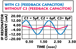
Figure 4 Plot of the resonator current for the 622 MHz crystal oscillator.
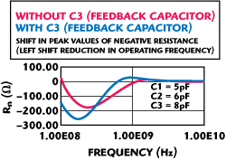
Figure 5 Plot of the input resistance Rn of the crystal oscillator.
UHF/VHF Crystal Oscillator Circuit
The resonance characteristic of the crystal resonator depends upon the thickness of the resonator. As the resonance frequency becomes higher, the crystal resonator becomes very thin and care must be taken to minimize the resonator drive level to avoid breakage of the resonator at high operating frequency. To avoid the breakdown phenomena of the crystal resonator at high frequency, one can opt for higher series resistance of the crystal that will restrict the level of the current accepted and returned from the crystal but at the cost of increased noise resistance associated with the series resistance RX.
Figure 3 shows conventional and modified Colpitts oscillator configurations for comparative analysis of drive level and negative resistance characteristics.6
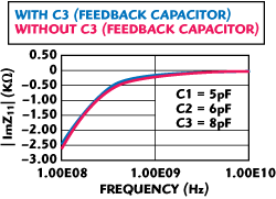
Figure 6 Plot of the input capacitance Cin of the crystal oscillator.
As illustrated, the feedback capacitor C3 of the modified topology is added to reduce the emitter voltage of the transistor, resulting in lower base current and drive level. Figures 4 and 5 show the plot of the resonator drive-level current and negative resistance of the conventional and modified Colpitts oscillators. The feedback capacitor C3 (C3 > C1) reduces the resonator current at steady state, but at the cost of shift in the peak value of the negative resistance. Therefore, this is a frequency limited approach. Figure 6 depicts the characteristics of the equivalent input capacitance of the crystal oscillator circuit. It can be seen that the value of the input capacitance is reduced; therefore, the circuit fails to oscillate at high frequency. In addition, the holder capacitance C0 of the crystal resonator influences the input impedance of the oscillator circuit in the UHF/VHF range, causing the C0 to perform at very low impedance at a high oscillation frequency.
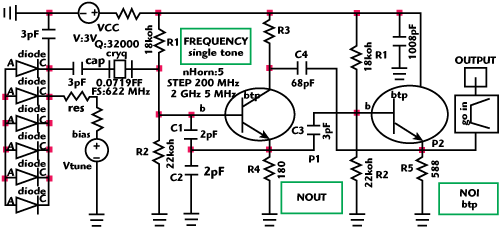
Figure 7 Example of a typical high frequency VCXO circuit (622 MHz).
Therefore, in order to apply the conventional circuit to the high frequency operation, it is necessary to obtain reasonably high value of negative resistance, while maintaining the equivalent input capacitance of the circuit. Figure 7 depicts the modified version of the Colpitts oscillator, in which the output signal from terminal P1 of the conventional Colpitts oscillator is fed through the capacitor C3 into the common-collector amplifier and brings the output signal from terminal P2 of the amplifier back into the collector through capacitor C4 of the conventional Colpitts oscillator.

Figure 8 Simulated input resistance of the typical high frequency VCXO circuit.
Figure 8 shows the plot of the equivalent input resistance of the modified Colpitts crystal oscillator circuit in comparison with the conventional Colpitts toplogy. It can be seen that negative resistance of the modified Colpitts oscillator at 622 MHz is typically twice as large as that of a conventional Colpitts oscillator circuit; therefore, it is suited for high frequency reference signal source applications. The drawback of this approach is the loading due to the feedback capacitor C4, which is compensated by connecting port P2 into the buffer amplifier for minimum load capacitance and power level variations.4
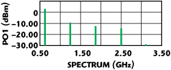
Figure 9 Simulated ouput power of the Colpitts oscillator.

Figure 10 Phase noise of the 622 MHz crystal oscillators.
Figure 9 shows the spurious characteristics of the 622 MHz VCXO. It can be seen that output response is a fundamental oscillation, therefore, free from sub-harmonics problems, which can be a major factor to deteriorate the jitter characteristic and phase noise performances of the VCXO. Figure 10 shows the phase noise plot of the conventional and modified Colpitts VCXO at 622 MHz. The typical phase noise plot of the modified version at a 10 kHz offset is 10 dB better than the conventional topology. However, the close-in phase noise performance (below 1 kHz offset) is the same.
Active Mode-Coupling Enables 622 MHz VCXO
Although the modified topology exhibits good phase noise performance at a far offset (> 1 kHz), it is still not superior to the commercially available 622 MHz SAW resonator-based oscillator. To overcome the phase noise problem, a novel VCXO circuit is proposed (see Figure 11) using an active mode-coupling mechanism that minimizes the jitter and phase, even those with relative low Q crystal resonators, for low phase noise and high frequency fundamental VCXO applications.
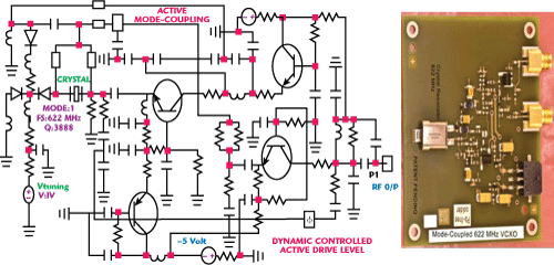
Figure 11 622 MHz active mode-coupled VCXO (patent pending).
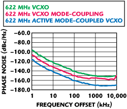
Figure 12 Typical measured phase noise of 622 MHz crystal oscillators.
Figure 12 shows that the typical measured phase noise at 10 kHz offset for a 622 MHz carrier frequency is -141 dBc/Hz, which is 10 to 15 dB superior to a commercially available 622 MHz SAW oscillator. At lower offset (1 Hz), the improvement in phase noise performance is limited due to the influence of the 1/f noise, which can be optimized by selecting a transistor that has low value of 1/f noise.
Conclusion
This work offers a cost-effective solution and can be applied for a crystal resonator (both high-Q and low-Q)-based VCXOs for substantial reduction in phase noise.
References
- E. Rubiola and V. Giordano, "On the 1/f Frequency Noise in Ultra-stable Quartz Oscillators," 2006 IEEE Frequency Control Symposium Digest, pp. 759-765.
- D.B. Leeson, "A Simple Model of Feedback Oscillator Noise Spectrum," IEEE Proceedings, Vol. 54, No. 2, 1966, pp. 329-332.
- S. Galliou, F. Sthal and M. Mourey, "Enhanced Phase Noise Model for Quartz Crystal Oscillators," 2002 IEEE Frequency Control Symposium Digest, pp. 627-632.
- N. Nomura, et al., "1 GHz High Frequency Colpitts Oscillator," 2005 IEEE Frequency Control Symposium Digest, pp. 1-4.
- N. Nomura, Y. Aoyagi and Y. Sekine, "A Colpitts-type Crystal Oscillator for Gigahertz Frequency," 2006 IEEE Frequency Control Symposium Digest, pp. 233-236.
- J. Matsuoka, T. Sato and T. Ohshima, "A Circuit for High Frequency Crystal Oscillators," Proceedings of the 2003 IEEE International Frequency Control Symposium and PDA Exhibition Jointly with the 17th European Frequency and Time Forum, pp. 569-574.
- Y Tsuzuki, T. Adachi and J.W. Zhang, "Fast Start-up Crystal Oscillator Circuits," 1995 IEEE Frequency Control Symposium Digest, pp. 565-568.
- Y Tsuzuki, T. Adachi and J.W. Zhang, "Formulation of Nonlinear Negative Resistance for Calculation of Start-up Characteristics of Crystal Oscillatorstor Circuits," 1996 IEEE Frequency Control Symposium Digest, pp. 710-713.
- Y Tsuzuki, T. Adachi and H. Yokohara, "Low Drive-level Crystal Oscillator Circuit," 1997 IEEE Frequency Control Symposium Digest, pp. 966-969.
- Y.S. Shmaliy, A.V. Marienko, O. Ibarra-Manzano and R. Rojas-Laguna, "Flicker Noise Conversion in Crystal Oscillator," Proceedings of the 2002 IEEE Frequency Control Symposium and PDA Exhibition, pp. 665-672.
- U.L. Rohde and A.K. Poddar, "Feedback and Mode-coupling Improves the Phase Noise Performances of the Crystal Oscillators," 2008 IEEE Frequency Control Symposium Digest, pp. 554-561.
- U.L. Rohde, A.K. Poddar and G. Boeck, Modern Microwave Oscillators for Wireless Applications: Theory and Optimization, John Wiley & Sons Inc., Somerset, NJ, 2005.