
The current trend towards increased data rates in mobile services has direct implications for the power amplifiers operating in these systems, which now need to be not only efficient but also wideband and, above all, linear. To operate efficiently, an amplifying device needs to see its optimum terminations at the input and output. Although basic amplifier theory suggests that an almost infinite number of harmonics need to be controlled to establish a particular device class of operation (such as (inv.) Class B, E, F),1 in practice, control of the fundamental, second and third harmonic is most of the time sufficient to achieve high performance. Furthermore, in order to operate linearly, the active device requires—in addition to a proper control at its fundamental and harmonic impedances—the correct baseband or envelope impedance, which, in the circuit implementation, is mostly determined by the biasing networks at the device input and output.
Since active devices operate in a large-signal/nonlinear mode when reaching high efficiency operation, the properties of the device under test (DUT) cannot simply be extrapolated from small-signal measurements. Consequently, active devices intended for large-signal operation need to be characterized under the exact same conditions as in their final application. To address this need, harmonic load-pull measurement systems have become a widely established tool. In these systems, the (harmonic) reflection coefficients offered to the device under test are "physically" varied to find the optimum (harmonic) loading conditions at the device input and output. With this optimum set of loading conditions the final matching circuit for the active device can be designed. Load-pull systems can be divided into two main categories: passive and active.

Figure 1 Typical load-pull configurations.
Passive Tuner-based Systems2,3
A typical passive load-pull configuration, shown in Figure 1a, makes use of sliding mechanical probes to tune the reflection coefficient. The bias tee placed after the tuner reduces the impact of its losses, but yields larger memory effects due to the baseband inductance. These kinds of systems are currently still the preferred industry large-signal test bench choice, due to their simplicity and high power handling capabilities. Unfortunately, passive load-pull setups are constrained by losses in the tuners, connecting cables and wafer probes, which limit the magnitude of the reflection coefficients that these systems can provide to the DUT.
Active Load-pull Systems
Active systems can, thanks to the use of amplifiers, overcome the reflection magnitude restrictions due to losses. Two main types of active systems can be identified, namely:
- Closed-loop active systems4 achieve their desired reflection coefficient by coupling out of the main path (using directional couplers) a portion of the wave generated by the DUT, adjusting it in amplitude and phase and then injecting it back as an incident wave to the active device (see Figure 1b). Here, the bias tee is placed as close as possible to the DUT to reduce unwanted memory effects. Since the injected signal is a direct function of the coupled wave, the loop gain and phase shift determine the reflection coefficient independently of power and spectral content of the signal. This makes the closed-loop concept suitable for fast device characterization, but also prone to oscillations since the loop gain cannot be very selectively controlled over frequency. To avoid the risk of oscillation, most closed-loop systems include sophisticated filtering.
- Open-loop active systems5 instead do not reuse the waves generated by the DUT, but directly inject a signal into the DUT, which is phase coherent with the input signal to the device, to compose a desired reflection coefficient (see Figure 1c). The desired reflection coefficient is created by adjusting the amplitude and phase of the injected wave. Here also, the bias tee is placed as close as possible to the DUT, to reduce the memory effects caused by bias path inductance. Since the injected signals are no longer a modified version of the waves generated by the DUT, the realized reflection coefficients are power and signal dependent. Therefore, iterations are needed during the measurements to find the optimal injection signals to offer the desired reflection coefficients to the DUT.

Figure 2 Phase delay caused by electrical lengths of cables/ adaptors/ probe.
Electrical Delay in Load-pull Systems
When working with modulated signals, for a well controlled linearity behavior of the DUT, the reflection coefficients offered to the DUT should ideally be constant (not vary versus frequency) within the modulation bandwidth at the fundamental, as well as in all related frequency bands at baseband and harmonic frequencies. This situation is approximated in real circuit implementations, where the matching networks are placed directly at the reference planes of the active device.

Figure 3 Reflection phase rotation at the DUT reference plane.
In conventional load-pull setups, however, the actual physical impedance is always located at some distance from the DUT (see Figure 2), which is much larger than for any practical matching network. This distance, as well as any physical length within the tuning element itself (such as the length of the active feedback loop, or the position of the probe in mechanical tuners), yields very large electrical delays causing rapid phase changes of the reflection coefficients versus frequency. Typical values for these phase fluctuations can vary from approximately 3°/MHz for a passive mechanical tuner to 30°/MHz in a conventional active closed-loop system (see Figure 3). Note that based on these values for a W-CDMA signal with adjacent and alternate channels (total bandwidth of 25 MHz), the reflection coefficient offered by a passive tuner would vary 75° in phase over this bandwidth, while in a conventional active closed-loop the phase change of the offered reflection coefficient would amount to 750°.
It is clear that these large phase deviations represent nonrealistic circuit conditions and will cause measurement errors such as IM3 asymmetry, spectral re-growth and EVM degradation. In general, maintaining the reflection coefficients constant over frequency is getting more and more difficult with the increase in modulation bandwidth of communication signals, not only in practical circuits, but definitely in load-pull measurement setups.

Figure 4 Principle of the proposed wideband open-loop active load-pull aproach.
Mixed-signal Load pull for Wideband Impedance Control
To overcome the aforementioned problems of losses and electrical delay in conventional load-pull characterization systems, while being able to work with realistic wideband communication signals, some major measurement system innovations are required. The principle of the proposed wideband open-loop active load-pull approach is shown in Figure 4. When the nonlinear DUT is excited with a user-defined modulated signal as, it generates signals in the baseband, fundamental and higher harmonic frequency bands. By measuring the device reflection coefficient at every frequency, the waves to be injected are estimated at every iteration. When the required reflection coefficient versus frequency (at every controlled band) is achieved, the iteration has converged and the large-signal parameters (that is power added efficiency, output power, intermodulation distortion, etc.) are measured. To address these needs a novel open-loop system was developed6 employing wideband signal generation and signal acquisition. A simplified block diagram of such a system is given in Figure 5.

Figure 5 Simplified schematic of the mixed-signal active open-loop load-pull system.
Signal Generation
When working with complex modulated signals, a good place to start is the modulation test standard.7,8 According to the test standard, a test signal is created, which consists of a finite sequence of IQ data samples specified in the time domain. In conventional lab instrumentation such as vector-signal generators, this sequence for a given standard (such as W-CDMA) is typically embedded in the instrument. In testing operation, these signals are uploaded in internal arbitrary waveform generators (AWG) and up-converted with IQ mixers yielding the modulated RF signal. In practice, these test records are sequentially repeated, yielding in the frequency domain a large but finite number of discrete spectral components. More precisely, the number of samples, in combination with the sampling speed at which the signal is generated, results in an effective frequency bin size (ΔƒAWG), or frequency resolution of the generated signal

where ΔƒAWG represents the frequency bin size of the generated signals, ƒsAWG and NAWG are respectively the sampling frequency and the number of samples used by the arbitrary waveform generators, and TMOD is the time period of the source signal that is needed to meet the requirements of the modulation standard according to the given test model.
To provide the reader with an example, a W-CDMA signal has a channel bandwidth of 5 MHz, a chip rate of 3.84 Mcps, 2560 chips/slot and 15 slots/frame. When considering one frame, the complex waveform is 10 ms long or, in other words, it will have a frequency resolution of 100 Hz. If then a single slot is considered, the frequency resolution becomes 1.5 kHz. This frequency representation allows one to analyze modulated communication signals like "classical" multi-tone signals, but now with a very large number of frequency tones.
Signal Acquisition
A fraction of the waves incident and reflected by the DUT is taken by the directional couplers and fed to high linearity mixers that down-convert the signals for digitization after which an FFT is applied to obtain their spectral content. Also here the sampling speed of the A/D converter and the time span used for the data-acquisition set an effective frequency bin size, which must be compatible with the original applied test signal, as described by the following expression

where ΔƒA/D is the resulting frequency bin size of the acquired signals, fsA/D and NA/D are respectively the sampling frequency and the number of samples used by the A/D converters, and k is an integer.
Controlling the Reflection Coefficients
When testing a nonlinear device with modulated signals, the measured waveforms will include not only the fundamental frequency band, but also the baseband, higher-order harmonics and intermodulation distortion products (see Figure 4). Since the reflection coefficient is defined as the ratio of two travelling waves, the effective control of the impedances over the whole modulation bandwidth offered to the DUT can be enforced by establishing the desired linear ratios of the incident and device generated waves on the DUT versus frequency. Or, in other words, a signal must be injected, at all the frequency components of interest, according to the linear relation,

in which ax,n and bx,n are the incident and reflected waves at port x and harmonic index n, while Γx,n represents the user defined reflection coefficient versus frequency for port x and harmonic index n. As in the classical open-loop approach, the new b-wave, containing all the frequency components of the signal of interest (that is more than 23000 frequency tones for a W-CDMA signal in a 35 MHz band), can be created from scratch, and any desired reflection coefficient behavior versus frequency can be created by adjusting the amplitude and phase of the injected waveform independently at each frequency component of interest.
Although conceptually simple, this method requires very fast highly linear data acquisition with high dynamic range to measure the reflection coefficients at every spectral component of the complex modulated signals with its related distortion products. Secondly, the a-waves need to be generated arbitrarily with a high dynamic range. Third, the signal injection at the various ports needs to be phase coherent at both the RF frequencies as well as at the baseband.
Practical Implementation
The block diagram of the system implementation is shown in Figure 5. The wideband reflection coefficients at the DUT reference planes are measured by coupling the traditional mixer-based super-heterodyne down-conversion used in conventional VNAs with wideband A/D converters (100 MHz sampling frequency). This hardware configuration enables the measurement of the device reflection coefficients over a wide bandwidth in a single data acquisition interval. Wider bandwidths, up to 120 MHz, can be measured by stepping the frequency of the local oscillator used for down-conversion.
The fundamental and harmonic frequency loads are synthesized by injecting fully coherent RF signals that are generated by IQ up-converted baseband signals, which are provided by (200 MS/s) arbitrary-waveform-generators (AWG). Custom bias tees with low inductance are placed directly at the DUT reference planes in order to minimize the electrical delay of the baseband (BB) impedance, implemented here as a passive impedance switch bank.9 On the baseband board also, the low-frequency couplers for the baseband impedance measurement are implemented. Note that in a more extended version, the baseband impedance can also be made active and controlled by an additional AWG.
Wideband Measurement Results and Comparison
To demonstrate the unique capabilities of the setup, a NXP Gen 6 LDMOS device with a gate width of 1.8 mm was measured. In the experiments, the drain current and voltage are set to 13 mA and 28 V, respectively. In this experiment, the optimum fundamental load and source matching conditions are found to be ΓL,f1 = |0.6|(Angle)45° and ΓS,f1=|0.5|(Angle)90°, while the input and output baseband impedances are set to a short condition. In addition, the input and output 2nd harmonics are set to circuit-like open conditions (ΓL,f2 = ΓS,f2 = |0.95|) to optimize the efficiency.
To highlight the excellent controllable bandwidth and the electrical delay-free operation of the new measurement setup, a comparison is made with a previously developed state-of-the-art active harmonic load-pull system,9 which was especially optimized for minimum electrical delay. For this purpose, a two-channel W-CDMA signal is used (centered at 2.135 and 2.145 GHz) and the input and output reflection coefficients in the newly developed setup are set to the following two cases:
- without electrical delay
- with an electrical delay of 4.85°/MHz for the fundamental source and load and 4.6°/MHz for the 2nd harmonic source and load

Figure 6 Source and load reflection coefficients at the device reference plane.
Figure 6 illustrates the source and load matching conditions in the fundamental (2.1225 to 2.1575 GHz) and harmonic (4.245 to 4.315 GHz) frequency range provided to the active device under test, with electrical delay (open symbols) and without electrical delay (filled symbols). Note that the filled markers represent the source and loading conditions for the two-carrier W-CDMA signal without any electrical delay, yielding completely overlapping points in the Smith chart. As shown in Figure 6, for the case with electrical delay, the fundament load trajectory has been shifted, such that the optimum matching condition is now centered at 2.135 GHz. This was required to avoid the unstable region of the active device.
It is important to note that this is a comparison to the "best possible case" of a classical closed-loop active load-pull system, since practical closed-loops will be subject to amplitude variations within the control frequency bands. Moreover, oscillation conditions in closed-loop systems for these very large bandwidths are difficult to avoid, due to the usage of wideband loop filters. Passive load-pull systems will have a comparable variation of the reflection coefficients versus frequency than the closed-loop system used in this comparison. The phase change can be even worse if high-Q resonators are used to control the harmonic terminations.


Figure 7 Measured output power spectral density vs. frequency of a NXP GEN6 LDMOS device: (a) at fundamental and (b) at second harmonic.
The measurement results are summarized in Table 1. There is significant performance degradation for the measured active device when the electrical delay is present in the reflection coefficients. This is also evident from Figure 7, which shows the power spectral density at the device output reference plane for the fundamental and 2nd harmonic frequency bands. Note that a 5 dB output power drop and close to 8 percent degradation of the power added efficiency (PAE) can be observed, when compared to the case with no electrical delay. It is important to stress that this performance degradation is a measurement artifact, the result of an incorrect measurement, which would mislead the user in judging the device performance.
Active Load Injection Power and Linearity
To provide the DUT with a specific ΓL, a certain injection power is needed, which not only depends on the output power of the DUT and the desired ΓL, but also on the output impedance of the device.10 When considering high-power devices, with output impedances in the order of few Ohms, the required injection power to cover the desired Smith chart area can be extremely high (2 to 10 times higher than the maximum output power of the DUT). To overcome this issue, typically, a pre-matching is used, which converts the 50 Ω impedance of the system to a value that is much closer to the output impedance of the DUT, thus reducing the power requirement of the load injection amplifier.
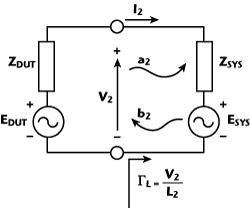
Figure 8 Thevenin equivalent schematic of an active load-pull configuration.
To give an example, a DUT with an output impedance of 2 Ω and an available output power of 200 W requires, when the system impedance is pre-matched to 10 Ω, an injection power of 360 W to synthesize a load impedance of 1 Ω. Reducing the system pre-matched impedance to 5 Ω lowers the required injection power for the same load condition to 142.2 W.
When considering multi-tone or modulated signals, the situation becomes more complicated as the linearity of the injection amplifier needs to be taken into account. To study the linearity constrains on the injection amplifier, consider a two-tone test signal, for which the power injected by the load amplifier at the IM3 frequencies of the two-tone test signal is given by

where ZDUT and Pb2,fund are the output impedance and the available power coming out of the DUT (see Figure 8). The load impedance offered to the DUT at the reference plane is varied by adjusting the equivalent voltage source ESYS in amplitude and phase. The related power needed to synthesize depends strongly on the equivalent system impedance ZSYS, which is the passive load impedance at the DUT reference plane; Pa2,fund and IP3,a2 are the power injected by the load amplifier and its output third-order intercept point, respectively.

Figure 9 Harmonic balance simulated IM3 level vs. output IP3.
Figure 9 shows the results of a harmonic balance simulation, where the apparent IM3 of the DUT versus decreasing output IP3 of the injection amplifier is shown for different pre-matching conditions of the system impedance. The dotted line is the actual IM3 level as would be achieved with passive matching techniques. The dot-dashed line represents the IM# level due to the Pa2,IM3 as approximated by Equation 1. A polynomial model was used for the amplifier linearity. In this experiment, the same DUT is used as for the single-tone considerations (Pavs = 200 W, output impedance = 2 Ω), which is set in the simulation to have an output IP3 of 63 dBm. For this device the output power is set equal to 50 W per tone, to have the same peak voltage as in the single-tone case. These conditions yield an actual IM3 of the DUT of -30.35 dBc. From Figure 9, it can be seen that this level (a correct measurement) is only achieved for sufficiently high IP3 of the injection amplifier. When the injection amplifier is less linear, it will introduce significant IM3 products, which can be approximated by Equation 4, and are also plotted in Figure 9. Note that IM3 cancelation effects can also occur. Consequently, to have reliable linearity measurements in a conventional active load-pull setup, even when pre-matching is used, the injection amplifier linearity (and thus its peak power) needs to be at least 10 times higher than that the of the DUT.
It is obvious that at high power, these amplifiers, if available, will be extremely expensive. For this reason, active load-pull systems that can offer communication standard compliant device testing, for example W-CDMA, at base station power levels (100 W and above) have not yet been demonstrated.

Figure 10 Measured load-pull contours of average power added efficiency and ACPR for an averaged output power of 30 W.
In a mixed-signal load-pull system, an iteration procedure is performed to obtain a user-defined reflection coefficient at each individual frequency component of a complex modulated signal, in and out of band. Due to these iterations, the injection amplifier is basically pre-distorted for its own nonlinearities, which allows the use of injection amplifiers with a much lower linearity than what is typically required in conventional active load-pull systems. As an example, consider Figure 10, which shows the ACPR and average PAE for a single-channel W-CDMA signal at 2.14 GHz, with a peak to average ratio of 9.5 dB. In these experiments the injection amplifier used has a maximum saturated power rating of only 200 W with an associated 60 dBm output IP3, while the reflection coefficient is controlled over a 35 MHz frequency span.
Conclusion
Mixed-signal techniques have been applied to extend the capabilities of traditional active load-pull setups. The realized system provides an unprecedented measurement speed, high dynamic range and is currently the only system that can handle communication standard compliant signals that are truly wideband such as multicarrier W-CDMA. The ability to eliminate losses and electrical delay, while being completely free in defining the source and load reflection coefficients versus frequency, allows perfect mimicking of in-circuit situations, making the system a tool of fundamental importance for the RF power amplifier developer.
References
- S.C. Cripps, RF Power Amplifier Design for Wireless Communications, Artech House Inc., Norwood, MA, 1999.
- Maury Microwave Application Note 5C-081, "Cascading Tuners for High-VSWR and Harmonic Load Pull," January 2009.
- C. Tsironis, R. Meierer, B. Hosein, T. Beauchamp and R. Jallad, "MPT, a Universal Multi-purpose Tuner," 2005 Automatic RF Techniques Group Conference Digest, pp. 113-117.
- G.P. Bava, U. Pisani and V. Pozzolo, "Active Load Technique for Load-pull Characterization at Microwave Frequencies," Electronic Letters, Vol. 18, No. 4, February 18, 1982, pp. 178-180.
- Y. Takayama, "A New Load-pull Characterization Method for Microwave Power Transistors," 1976 IEEE MTT-S International Microwave Symposium Digest, pp. 218-220.
- M. Marchetti, M. Pelk, K. Buisman, E. Neo, M. Spirito and L.C.N. de Vreede, "Active Harmonic Load Pull with Realistic Wideband Communication Signals," IEEE Transactions on Microwave Theory and Techniques, Vol. 56, No. 12, Part 2,†December 2008, pp. 2979-2988.
- 3GPP TS 25.104 V4.1.0 (2001-06), 3rd Generation Partnership Project; Technical Specification Group Radio Access Networks; UTRA (BS) FDD; Radio Transmission and Reception.
- 3GPP TS 25.141 V4.1.0 (2001-06), 3rd Generation Partnership Project; Technical Specification Group Radio Access Networks; Base station conformance testing (FDD)
- M. Spirito, M. Pelk, F. van Rijs, S.J.C.H. Theeuwen, D. Hartskeerl and L.C.N. de Vreede, "Active Harmonic Load Pull for On-wafer Out-of-band Device Linearity Optimization," IEEE Transactions on Microwave Theory and Techniques, Vol. 54, No. 12, Part 1, December 2006, pp. 4225-4236.
- Z. Aboush, C. Jones, G. Knight, A. Sheikh, H. Lee, J. Lees, J. Benedikt and P.J. Tasker, "High Power Active Harmonic Load-pull System for Characterization of High Power 100 W Transistors," 2005 European Microwave Conference Digest, pp. 609-612.